
User manual

...the world's most energy friendly microcontrollers
2012-04-24 - Giant Gecko Family - d0053_Rev0.96 229
www.energymicro.com
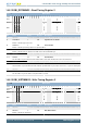
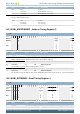
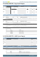
Bit Name Reset Access Description
Value Mode Description
0 RGB565 RGB data is 565.
1 RGB555 RGB data is 555.
23:22 Reserved
To ensure compatibility with future devices, always write bits to 0. More information in Section 2.1 (p. 3)
21:20 BANKSEL 0x0 RW Graphics Bank
This field sets the Memory Bank containing the Frame Buffer
Value Mode Description
0 BANK0 Memory bank 0 is used for Direct Drive, Masking, and Alpha Blending.
1 BANK1 Memory bank 1 is used for Direct Drive, Masking, and Alpha Blending.
2 BANK2 Memory bank 2 is used for Direct Drive, Masking, and Alpha Blending.
3 BANK3 Memory bank 3 is used for Direct Drive, Masking, and Alpha Blending.
19:17 Reserved
To ensure compatibility with future devices, always write bits to 0. More information in Section 2.1 (p. 3)
16 WIDTH 0 RW TFT Transaction Width
This field sets TFT tranaction width.
Value Mode Description
0 BYTE TFT Data is 8 bit wide.
1 HALFWORD TFT Data is 16 bit wide.
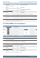
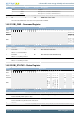
15:13 Reserved
To ensure compatibility with future devices, always write bits to 0. More information in Section 2.1 (p. 3)
12 COLOR1SRC 0 RW Masking/Alpha Blending Color1 Source
This field sets the Masking/Alpha Blending Color1 Source.
Value Mode Description
0 MEM Masking/Alpha Blending color 1 is read from external memory.
1 PIXEL1 Masking/Alpha Blending color 1 is read from EBI_TFTPIXEL1.
11:10 INTERLEAVE 0x0 RW Interleave Mode
This field sets the TFT Direct Drive Interleave mode.
Value Mode Description
0 UNLIMITED Allow unlimited interleaved EBI accesses per EBI_DCLK period. This can cause jitter
on the EBI_DCLK
1 ONEPERDCLK Allow 1 interleaved EBI access per EBI_DCLK period.
2 PORCH Only allow EBI accesses during TFT porches.
9 FBCTRIG 0 RW TFT Frame Base Copy Trigger
Sets the trigger on which the TFTFRAMEBASE is copied into an internal buffer. Direct Drive address generation is based on the
internal buffer.
Value Mode Description
0 VSYNC TFTFRAMEBASE is buffered on the vertical synchronization event EBI_VSYNC.
1 HSYNC TFTFRAMEBASE is buffered on the horizontal synchronization event EBI_HSYNC.
8 SHIFTDCLKEN 0 RW TFT EBI_DCLK Shift Enable
When this bit is set, EBI_DCLK edges are driven off the negative (instead of the positive) edge of the internal clock. SHIFTDCLKEN
is only allowed to be set to 1 if TFTHOLD in EBI_TFTTIMING is at least 1.
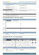
7:5 Reserved
To ensure compatibility with future devices, always write bits to 0. More information in Section 2.1 (p. 3)
4:2 MASKBLEND 0x0 RW TFT Mask and Blend Mode
This field sets the Mask and Blend Mode.
Value Mode Description
0 DISABLED Masking and Blending are disabled.
1 IMASK Internal Masking is enabled.
2 IALPHA Internal Alpha Blending is enabled.
3 IMASKIALPHA Internal Masking and Alpha Blending are enabled.
5 EMASK External Masking is enabled.
6 EALPHA External Alpha Blending is enabled.