
User manual


...the world's most energy friendly microcontrollers
2012-04-24 - Giant Gecko Family - d0053_Rev0.96 191
www.energymicro.com
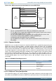
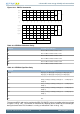
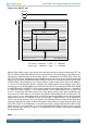
Figure 14.26. EBI Connection with Chip Enable Don't Care NAND Flash
EBI
(EFM32)
CE don’t care
NAND
Flash
GPIO
CLE
ALE
R/B
CEn
WPn
IO[]
WEn
REn
EBI_NANDREn
(2)
GPIO
(4)
EBI_CSn
EBI_A[25]
(1)
EBI_A[24]
(1)
EBI_NANDWEn
(2)
EBI_AD[]
(3)
Note
• (0) For a standard NAND Flash the EBI_CSn should be left unconnected.
• (1) The address lines mapping to the NAND Flash ALE and CLE signals can be chosen
as explained in Section 14.3.14.1 (p. 191)
• (2) For a CEDC NAND Flash the shared EBI_REn and EBI_WEn pins can be used
instead of the dedicated EBI_NANDREn and EBI_NANDWEn pins
• (3) Both 8-bit and 16-bit NAND Flash are supported.
• (4) The NAND Flash ready/busy (R/B) signal should be observed via GPIO (not via
EBI_ARDY)
14.3.14.1 Register Selection
NAND Flash uses an indirect I/O interface in which the NAND Flash is controlled by programming the
NAND Flash internal Command, Address, and Data registers. NAND Flash does not use dedicated
address lines. Because of this indirect I/O interface the NAND Flash memory size is not restricted by the
memory map of the EFM32GG. The NAND Command, Address, and Data registers can be accessed
via memory mapped IO in which two address lines are chosen for connection with the ALE and CLE
signals. The memory mapping and the two used address lines should be chosen such that they adhere
to the ALE/CLE encoding shown in Table 14.4 (p. 191) . Either EBI_A or EBI_AD address lines can
be used as long as the chosen addressing mode does not multiplex data signals onto the chosen lines.
The EBI_A[25:24] address lines used in Figure 14.25 (p. 190) and Figure 14.26 (p. 191) are just
an example.
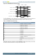
Table 14.4. EBI NAND Flash Register Select
ALE CLE Selected NAND Flash Register
0 0 Data Register
0 1 Command Register
1 0 Address Register
1 1 Undefined
14.3.14.2 Width and Timing Configuration
The regular EBI registers are used for defining transfer width, read timing, and write timing for the
transactions on the NAND Flash interface. NAND Flash specific parameters as for example block size or