
User manual

...the world's most energy friendly microcontrollers
2012-04-24 - Giant Gecko Family - d0053_Rev0.96 171
www.energymicro.com
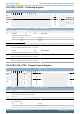
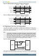
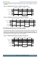
13.5.3 PRS_ROUTE - I/O Routing Register
Offset Bit Position
0x008
31
30
29
28
27
26
25
24
23
22
21
20
19
18
17
16
15
14
13
12
11
10
9
8
7
6
5
4
3
2
1
0
Reset
0x0
0
0
0
0
Access
RW
RW
RW
RW
RW
Name
LOCATION
CH3PEN
CH2PEN
CH1PEN
CH0PEN
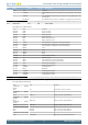
Bit Name Reset Access Description
31:11 Reserved
To ensure compatibility with future devices, always write bits to 0. More information in Section 2.1 (p. 3)
10:8 LOCATION 0x0 RW I/O Location
Decides the location of the PRS I/O pins.
Value Mode Description
0 LOC0 Location 0
1 LOC1 Location 1
7:4 Reserved
To ensure compatibility with future devices, always write bits to 0. More information in Section 2.1 (p. 3)
3 CH3PEN 0 RW CH3 Pin Enable
When set, GPIO output from PRS channel 3 is enabled
2 CH2PEN 0 RW CH2 Pin Enable
When set, GPIO output from PRS channel 2 is enabled
1 CH1PEN 0 RW CH1 Pin Enable
When set, GPIO output from PRS channel 1 is enabled
0 CH0PEN 0 RW CH0 Pin Enable
When set, GPIO output from PRS channel 0 is enabled
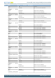
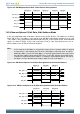
13.5.4 PRS_CHx_CTRL - Channel Control Register
Offset Bit Position
0x010
31
30
29
28
27
26
25
24
23
22
21
20
19
18
17
16
15
14
13
12
11
10
9
8
7
6
5
4
3
2
1
0
Reset
0
0x0
0x00
0x0
Access
RW
RW
RW
RW
Name
ASYNC
EDSEL
SOURCESEL
SIGSEL
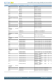
Bit Name Reset Access Description
31:29 Reserved
To ensure compatibility with future devices, always write bits to 0. More information in Section 2.1 (p. 3)
28 ASYNC 0 RW Asynchronous reflex
Set to disable synchronization of this reflex signal
27:26 Reserved
To ensure compatibility with future devices, always write bits to 0. More information in Section 2.1 (p. 3)
25:24 EDSEL 0x0 RW Edge Detect Select
Select edge detection.
Value Mode Description
0 OFF Signal is left as it is