...
...the world's most energy friendly microcontrollers 1 Energy Friendly Microcontrollers 1.1 Typical Applications The EFM32GG Giant Gecko is the ideal choice for demanding 8-, 16-, and 32-bit energy sensitive applications. The devices are developed to minimise the product of power and time over all phases of MCU operation.
...the world's most energy friendly microcontrollers 2 About This Document This document contains reference material for the EFM32GG series of microcontrollers. All modules and peripherals in the EFM32GG series devices are described in general terms. Not all modules are present in all devices and the feature set for each device might vary. Such differences, including pinout, are covered in the device-specific datasheets. 2.
...the world's most energy friendly microcontrollers Registers and bit fields marked with reserved are reserved for future use. These should be written to 0 unless otherwise stated in the Register Description. Reserved bits might be read as 1 in future devices. Reset Value The reset value denotes the value after reset. Registers denoted with X have unknown value out of reset and need to be initialized before use.
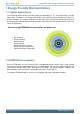
...the world's most energy friendly microcontrollers 3 System Overview 3.1 Introduction The EFM32 MCUs are the world’s most energy friendly microcontrollers. With a unique combination of the powerful 32-bit ARM Cortex-M3, innovative low energy techniques, short wake-up time from energy saving modes, and a wide selection of peripherals, the EFM32GG microcontroller is well suited for any battery operated application as well as other systems requiring high performance and low-energy consumption, see Figure 3.
...
...the world's most energy friendly microcontrollers Figure 3.1. Diagram of EFM32GG Giant Gecko Core and Mem ory Clock Managem ent Mem ory Prot ect ion Unit ARM Cort ex™-M3 processor Flash Program Mem ory Debug Int erface w/ ETM RAM Mem ory Energy Managem ent High Freq. Cryst al Oscillat or High Freq. RC Oscillat or Volt age Regulat or Volt age Com parat or Low Freq. Cryst al Oscillat or Low Freq. RC Oscillat or Brown-out Det ect or Power-on Reset Ult ra Low Freq.
...the world's most energy friendly microcontrollers Table 3.1. Energy Mode Description Energy Mode Name Description EM0 – Energy Mode 0 0 1 2 3 0 1 2 3 0 1 2 3 0 1 2 3 (Run mode) In EM0, the CPU is running and consuming as little as 200 µA/MHz, when running code from flash. All peripherals can also be activated. EM1 – Energy Mode 1 (Sleep Mode) In EM1, the CPU is sleeping and the power consumption is only 50 µA/MHz . The peripherals including, DMA, PRS and memory system is still available.
GPIO(pins) USB LCD USART+UART LEUART LETIMER RTC PCNT Watchdog ADC(pins) DAC(pins) ACMP(pins) AES EBI LESENSE Op-Amps Package 512 128 86 - - 3+2 2 2 4 (12) 1 1 3 1 1 (8) 2 (2) 2 (16) Y Y 3 Y LQFP100 280F1024 1024 128 86 - - 3+2 2 2 4 (12) 1 1 3 1 1 (8) 2 (2) 2 (16) Y Y 3 Y LQFP100 290F512 512 128 90 - - 3+2 2 2 4 (12) 1 1 3 1 1 (8) 2 (2) 2 (16) Y Y 3 Y LFBGA112 290F1024 1024 128 90 - - 3+2 2 2 4 (12) 1 1 3 1 1 (8)
USB LCD USART+UART LEUART LETIMER RTC PCNT Watchdog ADC(pins) DAC(pins) ACMP(pins) AES EBI LESENSE Op-Amps 128 53 Y 8x18 3 2 2 4 (12) 1 1 3 1 1 (8) 2 (2) 1 (4) Y - 3 Y QFN64 940F1024 1024 128 53 Y 8x18 3 2 2 4 (12) 1 1 3 1 1 (8) 2 (2) 1 (4) Y - 3 Y QFN64 942F512 512 128 50 Y 8x16 3 2 2 4 (11) 1 1 3 1 1 (8) 2 (2) 1 (4) Y - 3 Y TQFP64 942F1024 1024 128 50 Y 8x16 3 2 2 4 (11) 1 1 3 1 1 (8) 2 (2) 1 (4) Y - 3 Y TQFP
...the world's most energy friendly microcontrollers 4 System Processor Quick Facts What? 0 1 2 3 4 The industry leading Cortex-M3 processor from ARM is the CPU in the EFM32GG microcontrollers. Why? CM 3 Cor e The ARM Cortex-M3 is designed for exceptional short response time, high code density, and high 32-bit throughput while maintaining a strict cost and power consumption budget.
...
...the world's most energy friendly microcontrollers IRQ # Table 4.1.
...the world's most energy friendly microcontrollers 5 Memory and Bus System Quick Facts What? 0 1 2 3 A low latency memory system including low energy Flash and RAM with data retention which makes the energy modes attractive. 4 Why? Fla sh RAM retention reduces the need for storing data in Flash and enables frequent use of the ultra low energy modes EM2 and EM3 with as little as 0.9 µA µA current consumption.
...the world's most energy friendly microcontrollers Figure 5.1. EFM32GG Bus System Cort ex-M3 ICode Flash AHB Mult ilayer Bus Mat rix RAM EBI DCode AES Syst em AHB/ APB Bridge Peripheral 0 DMA Peripheral n 5.2 Functional Description The memory segments are mapped together with the internal segments of the Cortex-M3 into the system memory map shown by Figure 5.2 (p. 15) Figure 5.2. System Address Space 2012-04-24 - Giant Gecko Family - d0053_Rev0.96 15 www.energymicro.
...the world's most energy friendly microcontrollers The embedded SRAM is located at address 0x20000000 in the memory map of the EFM32GG. When running code located in SRAM starting at this address, the Cortex-M3 uses the System bus interface to fetch instructions. This results in reduced performance as the Cortex-M3 accesses stack, other data in SRAM and peripherals using the System bus interface. To be able to run code from SRAM efficiently, the SRAM is also mapped in the code space at address 0x10000000.
...the world's most energy friendly microcontrollers Table 5.1.
...the world's most energy friendly microcontrollers Table 5.2.
...the world's most energy friendly microcontrollers Table 5.3.
...the world's most energy friendly microcontrollers 5.2.3.1 Arbitration The Bus Matrix uses a round-robin arbitration algorithm which enables high throughput and low latency while starvation of simultaneous accesses to the same bus slave are eliminated. Round-robin does not assign a fixed priority to each bus master. The arbiter does not insert any bus wait-states. 5.2.3.
...the world's most energy friendly microcontrollers All Low Energy Peripherals are memory mapped, with automatic data synchronization. Because the Low Energy Peripherals are running on clocks asynchronous to the core clock, there are some constraints on how register accesses are performed, as described in the following sections. 5.3.1.
...the world's most energy friendly microcontrollers immediately on the peripheral write access. If such a write is done close to an edge on the clock of the peripheral, the write is delayed to after the clock edge. This will introduce wait-states on the peripheral access. On peripherals with delayed synchronization, the SYNCBUSY registers are still present.
...the world's most energy friendly microcontrollers starting the synchronization process, thus providing precise control of the module update process. The synchronization process is started by clearing the REGFREEZE bit. Note The FREEZE register is also present on peripherals with immediate synchronization, but there it has no effect 5.4 Flash The Flash retains data in any state and typically stores the application code, special user data and security information.
...
...the world's most energy friendly microcontrollers DI Address Register Description 0x0FE081F8 MEM_INFO_FLASH [15:0]: Flash size, kbyte count as unsigned integer (eg. 128) 0x0FE081FA MEM_INFO_RAM [15:0]: Ram size, kbyte count as unsigned integer (eg. 16) 0x0FE081FC PART_NUMBER [15:0]: EFM32 part number as unsigned integer (eg.
...the world's most energy friendly microcontrollers 6 DBG - Debug Interface Quick Facts What? 0 1 2 3 4 The DBG (Debug Interface) is used to program and debug EFM32GG devices. Why? The Debug Interface makes it easy to reprogram and update the system in field, and allows debugging with minimal I/O pin use. ARM Cor t e x-M 3 How? D BG Debug Dat a The Cortex-M3 supports advanced debugging features. EFM32GG devices only use two port pins for debugging or programming.
...the world's most energy friendly microcontrollers For more information on how to enable the debug pin outputs/inputs the reader is referred to Section 32.3.4.1 (p. 753) , the ARM Cortex-M3 Technical Reference Manual and the ARM CoreSight Technical Reference Manual Note Leaving the debug pins enabled will lead to an increase in current consumption in EM2EM4 6.3.2 Embedded Trace Macrocell v3.5 (ETM) The ETM makes it possible to trace both instruction and data from the processor in real time.
...the world's most energy friendly microcontrollers Figure 6.2. Device Unlock Reset Locked No access APP Program execut ion 150 us Unlocked No access APP Cort ex Program execut ion 47 us Ext ended unlocked No access Ext ended APP Cort ex 255 x 47 us Figure 6.3. APP Expansion swdio swclk app_expand The device is unlocked by writing to the AAP_CMDKEY register and then setting the DEVICEERASE bit of the AAP_CMD register via the debug interface.
...the world's most energy friendly microcontrollers 6.5 Register Map The offset register address is relative to the registers base address. Offset Name Type Description 0x000 AAP_CMD W1 Command Register 0x004 AAP_CMDKEY W1 Command Key Register 0x008 AAP_STATUS R Status Register 0x0FC AAP_IDR R AAP Identification Register 6.6 Register Description 6.6.
...the world's most energy friendly microcontrollers Bit Name Reset Access Description The key value must be written to this register to write enable the AAP_CMD register. Value Mode Description 0xCFACC118 WRITEEN Enable write to AAP_CMD 6.6.
...the world's most energy friendly microcontrollers 7 MSC - Memory System Controller Quick Facts What? The user can perform Flash memory read, read configuration and write operations through the Memory System Controller (MSC) . Why? 0 1 2 3 The MSC allows the application code, user data and flash lock bits to be stored in nonvolatile Flash memory.
...the world's most energy friendly microcontrollers divided into two blocks; the main block and the information block. Program code is normally written to the main block. Additionally, the information block is available for special user data and flash lock bits. There is also a read-only page in the information block containing system and device calibration data. Read and write operations are supported in the energy modes EM0 and EM1. 7.
...the world's most energy friendly microcontrollers Table 7.1. MSC Flash Memory Mapping Block 1 Main Page Base address Write/Erase by Software readable Purpose/Name Size 0 0x00000000 Software, debug Yes User code and data 512 KB - 1024 KB Software, debug Yes .
...the world's most energy friendly microcontrollers There are 32 page lock bits per page lock word (PLW). Bit 0 refers to the first page and bit 31 refers to the last page within a PLW. Thus, PLW[0] contains lock bits for page 0-31 in the main block, PLW[1] contains lock bits for page 32-63 etc. A page is locked when the bit is 0. A locked page cannot be erased or written. Word 127 is the debug lock word (DLW). The four LSBs of this word are the debug lock bits.
...the world's most energy friendly microcontrollers is undefined. If a HFCORECLK frequency above 16 MHz is to be set by software, the MODE field of the MSC_READCTRL register must be set to WS1 or WS1SCBTP before the core clock is switched to the higher frequency clock source. When changing to a lower frequency, the MODE field of the MSC_READCTRL register must be set to WS0 or WS0SCBTP only after the frequency transition has completed.
...the world's most energy friendly microcontrollers is returned to the processor in one clock cycle. Thus, performance is also improved when wait-states are used (i.e. running at frequencies above 16 MHz). The instruction cache is connected directly to the ICODE bus on the Cortex-M3 and functions as a memory access filter between the processor and the memory system, as illustrated in Figure 7.2 (p. 36) .
...the world's most energy friendly microcontrollers cache misses occur inside the interrupt routine. So, for example, if a cached function is called from the interrupt routine, the instructions for that function will be taken from the cache. The cache content is not retained in EM2, EM3 and EM4. The cache is therefore invalidated regardless of the setting of AIDIS in MSC_READCTRL when entering these energy modes.
...the world's most energy friendly microcontrollers • Write 0xFFFFAAAA (word in flash becomes 0xFFFFAAAA) • Write 0x5555FFFF (word in flash becomes 0x5555AAAA) Note During a write or erase, flash read accesses not subject to read-while-write will be stalled, effectively halting code execution from flash. Code execution continues upon write/ erase completion. Code residing in RAM may be executed during a write/erase operation regardless of whether read-while-write is enabled or not. 7.3.6.
...the world's most energy friendly microcontrollers 7.4 Register Map The offset register address is relative to the registers base address.
...the world's most energy friendly microcontrollers 7.5.2 MSC_READCTRL - Read Control Register Access 0 2 1 RW 0x1 MODE 3 RW IFCDIS 0 4 RW AIDIS 0 5 6 RW 0 7 ICCDIS 0 RW 0 0 RW RAMCEN EBICDIS Name PREFETCH BUSSTRATEGY Access RW Reset 8 9 10 11 12 13 14 15 16 17 RW 0x0 18 19 20 21 22 23 24 25 26 27 28 29 30 0x004 Bit Position 31 Offset Bit Name Reset Description 31:18 Reserved To ensure compatibility with future devices, always write bits to 0.
...the world's most energy friendly microcontrollers Bit Name Reset Access Description Value Mode Description 4 WS2 Two wait-states inserted for eatch fetch or read transfer. This mode is required for a core frequency above 32 MHz 5 WS2SCBTP Two wait-state access with SCBTP enabled. 7.5.
...the world's most energy friendly microcontrollers Bit Name Reset Access Description 12 CLEARWDATA 0 W1 Clear WDATA state Will set WDATAREADY and DMA request. Should only be used when no write is active. 11:10 Reserved To ensure compatibility with future devices, always write bits to 0. More information in Section 2.1 (p. 3) 9 ERASEMAIN1 0 W1 Mass erase region 1 Initiate mass erase of region 1. For devices supporting read-while-write, this is the upper half of the flash.
...the world's most energy friendly microcontrollers 7.5.6 MSC_WDATA - Write Data Register 0 1 2 3 4 5 6 7 8 9 10 11 12 13 14 15 16 0x00000000 17 18 19 20 21 22 23 24 25 26 27 28 29 30 0x018 Bit Position 31 Offset RW Reset WDATA Access Name Bit Name Reset Access Description 31:0 WDATA 0x00000000 RW Write Data The data to be written to the address in MSC_ADDR.
...the world's most energy friendly microcontrollers Bit Name Reset Access Description When set, the last erase or write is aborted due to erase/write access constraints 0 BUSY 0 R Erase/Write Busy When set, an erase or write operation is in progress and new commands are ignored 7.5.
...the world's most energy friendly microcontrollers Bit Name Reset Access Description 0 ERASE 0 W1 Erase Done Interrupt Set Set the erase done bit and generate interrupt 7.5.
...the world's most energy friendly microcontrollers Bit Name Reset Access Description Enable the erase done interrupt 7.5.12 MSC_LOCK - Configuration Lock Register 0 1 2 3 4 5 6 7 8 0x0000 9 10 11 12 13 14 15 16 17 18 19 20 21 22 23 24 25 26 27 28 29 30 0x03C Bit Position 31 Offset RW Reset LOCKKEY Access Name Bit Name Reset Access Description 31:16 Reserved To ensure compatibility with future devices, always write bits to 0.
...the world's most energy friendly microcontrollers 7.5.14 MSC_CACHEHITS - Cache Hits Performance Counter 0 1 2 3 4 5 6 7 8 9 10 0x00000 11 12 13 14 15 16 17 18 19 20 21 22 23 24 25 26 27 28 29 30 0x044 Bit Position 31 Offset Reset CACHEHITS R Access Name Bit Name Reset Access Description 31:20 Reserved To ensure compatibility with future devices, always write bits to 0. More information in Section 2.1 (p.
...the world's most energy friendly microcontrollers Bit Name Reset Access Description 31:17 Reserved To ensure compatibility with future devices, always write bits to 0. More information in Section 2.1 (p.
...the world's most energy friendly microcontrollers 8 DMA - DMA Controller Quick Facts What? 0 1 2 3 4 The DMA controller can move data without CPU intervention, effectively reducing the energy consumption for a data transfer. Why? Flash The DMA can perform data transfers more energy efficiently than the CPU and allows autonomous operation in low energy modes.
...
...the world's most energy friendly microcontrollers • A channel select block routing the right peripheral request to each DMA channel 8.4 Functional Description The DMA Controller is highly flexible. It is capable of transferring data between peripherals and memory without involvement from the processor core.
...the world's most energy friendly microcontrollers 4 and this determines the arbitration rate. For example, if R = 4 then the arbitration rate is 2 , that is, the controller arbitrates every 16 DMA transfers. Table 8.1 (p. 52) lists the arbitration rates. Table 8.1.
...
...the world's most energy friendly microcontrollers Figure 8.2. Polling flowchart St art polling Is t here a channel request ? N o Yes Are any channel request s using a high priorit ylevel ? No Yes Select channel t hat has t he lowest channel num ber and is set t o high priorit y-level Select channel t hat has t he lowest channel num ber St art DMA t ransfer 8.4.2.3 DMA cycle types The cycle_ctrl bits control how the controller performs a DMA cycle. You can set the cycle_ctrl bits as Table 8.
...the world's most energy friendly microcontrollers DMA transfer completes. Therefore, you must take care when setting the R_power, that you do not significantly increase the latency for high-priority channels. 8.4.2.3.1 Invalid After the controller completes a DMA cycle it sets the cycle type to invalid, to prevent it from repeating the same DMA cycle. 8.4.2.3.2 Basic In this mode, you configure the controller to use either the primary, or alternate, data structure.
...the world's most energy friendly microcontrollers Figure 8.3.
...the world's most energy friendly microcontrollers 9. The controller performs four DMA transfers. 10.The controller arbitrates. After the controller receives a request for this channel, the flow continues if the channel has the highest priority. 11.The controller performs the remaining four DMA transfers. 12.The controller sets dma_done[C] HIGH for one HFCORECLK cycle and enters the arbitration process. After task B completes, the host processor can configure the alternate data structure for task D.
...the world's most energy friendly microcontrollers using the primary data structure. The controller continues to switch from primary to alternate to primary… until either: • the host processor configures the alternate data structure for a basic cycle • it reads an invalid data structure. Note After the controller completes the N primary transfers it invalidates the primary data structure by setting the cycle_ctrl field to b000.
...the world's most energy friendly microcontrollers Figure 8.4. Memory scatter-gather example Init ializat ion:1. Configure prim ary t o enable t he copy A, B, C, and D operat ions: cycle_ct rl = b100, 2 R = 4, N = 16. 2. Writ e t he prim ary source dat a t o m em ory, using t he st ruct ure shown in t he following t able.
...the world's most energy friendly microcontrollers 8. The controller generates an auto-request for the channel and then arbitrates. 9. The controller performs task C. After it completes the task, it generates an auto-request for the channel and then arbitrates. 10.The controller performs four DMA transfers. These transfers write the alternate data structure for task D. 11.The controller sets the cycle_ctrl bits of the primary data structure to b000, to indicate that this data structure is now invalid. 12.
...the world's most energy friendly microcontrollers Bit Field Value [13:4] n_minus_1 N [3] next_useburst - Description 1 Configures the controller to perform N DMA transfers, where N is a multiple of four When set to 1, the controller sets the chnl_useburst_set [C] bit to 1 after the alternate transfer completes 1 Because the R_power field is set to four, you must set N to be a multiple of four. The value given by N/4 is the number of times that you must configure the alternate data structure.
...the world's most energy friendly microcontrollers Primary, copy A Task A 1. After receiving a request, the controller performs four DMA transfers. These transfers write the alternate data structure for task A. 2. The controller performs task A. 3. After the controller completes the task it enters the arbitration process. After the peripheral issues a new request and it has the highest priority then the process continues with: Primary, copy B Task B 4. The controller performs four DMA transfers.
...the world's most energy friendly microcontrollers • have a base address that is an integer multiple of the total size of the channel control data structure. Figure 8.6 (p. 63) shows the memory that the controller requires for the channel control data structure, when all 12 channels and the optional alternate data structure are in use. Figure 8.6.
...the world's most energy friendly microcontrollers Figure 8.7.
...the world's most energy friendly microcontrollers 8.4.3.2 Destination data end pointer The dst_data_end_ptr memory location contains a pointer to the end address of the destination data. Table 8.8 (p. 65) lists the bit assignments for this memory location. Table 8.8.
...the world's most energy friendly microcontrollers Bit Name Description Note You must set dst_size to contain the same value that src_size contains. [27:26] src_inc Set the bits to control the source address increment. The address increment depends on the source data width as follows: Source data width = byte b00 = byte. b01 = halfword. b10 = word. Source data width = halfword b11 = no increment. Address remains set to the value that the src_data_end_ptr memory location contains. b00 = reserved.
...the world's most energy friendly microcontrollers Bit Name Description [13:4] n_minus_1 Prior to the DMA cycle commencing, these bits represent the total number of DMA transfers that the DMA cycle contains. You must set these bits according to the size of DMA cycle that you require. The 10-bit value indicates the number of DMA transfers, minus one.
...the world's most energy friendly microcontrollers Bit Name Description When the controller operates in peripheral scatter-gather mode, you must only use this value in the alternate data structure. R At the start of a DMA cycle, or 2 DMA transfer, the controller fetches the channel_cfg from system R memory. After it performs 2 , or N, transfers it stores the updated channel_cfg in system memory. The controller does not support a dst_size value that is different to the src_size value.
...the world's most energy friendly microcontrollers Table 8.11.
...the world's most energy friendly microcontrollers set SRCSTRIDE in DMA_RECT0 to the outer rectangle width of the source, and DSTSTRIDE in DMA_RECT0 to the outer rectangle width of the destination rectangle. Finally, the channel descriptor for channel 0 has to be configured. The source and destination end pointers should be set to the last element of the first line of the source data and destination data respectively.
...the world's most energy friendly microcontrollers individual DMA channels remember source and destination end pointers while active, speeding up their transfers. 8.4.6 Interaction with the EMU The DMA interacts with the Energy Management Unit (EMU) to allow transfers from e.g. the LEUART to occur in EM2. The EMU can wake up the DMA sufficiently long to allow data transfers to occur. See section "DMA Support" in the LEUART documentation. 8.4.
...the world's most energy friendly microcontrollers 8.6 Register Map The offset register address is relative to the registers base address.
...the world's most energy friendly microcontrollers 8.7 Register Description 8.7.1 DMA_STATUS - DMA Status Registers R 0 0 1 2 3 4 5 0x0 Access EN Name STATE CHNUM R Access R Reset 6 7 8 9 10 11 12 13 14 15 16 17 18 0x0B 19 20 21 22 23 24 25 26 27 28 29 30 0x000 Bit Position 31 Offset Bit Name Reset Description 31:21 Reserved To ensure compatibility with future devices, always write bits to 0. More information in Section 2.1 (p.
...the world's most energy friendly microcontrollers Bit Name Reset Access Description 5 CHPROT 0 W Channel Protection Control Control whether accesses done by the DMA controller are privileged or not. When CHPROT = 1 then HPROT is HIGH and the access is privileged. When CHPROT = 0 then HPROT is LOW and the access is non-privileged. 4:1 Reserved To ensure compatibility with future devices, always write bits to 0. More information in Section 2.1 (p.
...the world's most energy friendly microcontrollers Bit Name Reset Access Description The base address of the alternate data structure. This register will read as DMA_CTRLBASE + 0x100. 8.7.
...the world's most energy friendly microcontrollers 8.7.
...the world's most energy friendly microcontrollers 8.7.
...the world's most energy friendly microcontrollers 8.7.
...the world's most energy friendly microcontrollers 8.7.
...the world's most energy friendly microcontrollers 8.7.
...the world's most energy friendly microcontrollers 8.7.
...the world's most energy friendly microcontrollers Bit Name Reset Access Description 31:12 Reserved To ensure compatibility with future devices, always write bits to 0. More information in Section 2.1 (p. 3) 11 CH11ENC 0 W1 Channel 11 Enable Clear Write to 1 to disable this channel. See also description for channel 0. 10 CH10ENC 0 W1 Channel 10 Enable Clear Write to 1 to disable this channel. See also description for channel 0.
...the world's most energy friendly microcontrollers Bit Name Reset Access Description Write to 1 to select the alternate structure for this channel. 8 CH8ALTS 0 RW1 Channel 8 Alternate Structure Set Write to 1 to select the alternate structure for this channel. 7 CH7ALTS 0 RW1 Channel 7 Alternate Structure Set Write to 1 to select the alternate structure for this channel. 6 CH6ALTS 0 RW1 Channel 6 Alternate Structure Set Write to 1 to select the alternate structure for this channel.
...the world's most energy friendly microcontrollers Bit Name Reset Access Description 5 CH5ALTC 0 W1 Channel 5 Alternate Clear Write to 1 to select the primary structure for this channel. 4 CH4ALTC 0 W1 Channel 4 Alternate Clear Write to 1 to select the primary structure for this channel. 3 CH3ALTC 0 W1 Channel 3 Alternate Clear Write to 1 to select the primary structure for this channel.
...the world's most energy friendly microcontrollers Bit Name Reset Access Description Write to 1 to obtain high priority for this channel. Reading returns the channel priority status. 1 CH1PRIS 0 RW1 Channel 1 High Priority Set Write to 1 to obtain high priority for this channel. Reading returns the channel priority status. 0 CH0PRIS 0 RW1 Channel 0 High Priority Set Write to 1 to obtain high priority for this channel. Reading returns the channel priority status. 8.7.
...the world's most energy friendly microcontrollers 8.7.17 DMA_ERRORC - Bus Error Clear Register RW 0 Reset 0 1 2 3 4 5 6 7 8 9 10 11 12 13 14 15 16 17 18 19 20 21 22 23 24 25 26 27 28 29 30 0x04C Bit Position 31 Offset ERRORC Access Name Bit Name Reset Access Description 31:1 Reserved To ensure compatibility with future devices, always write bits to 0. More information in Section 2.1 (p.
...the world's most energy friendly microcontrollers Bit Name Reset Access Description 5 CH5REQSTATUS 0 R Channel 5 Request Status When this bit is 1, it indicates that the peripheral connected as the input to this DMA channel is requesting the controller to service R the DMA channel. The controller services the request by performing the DMA cycle using 2 DMA transfers.
...the world's most energy friendly microcontrollers Bit Name Reset Access Description When this bit is 1, it indicates that the peripheral connected as the input to this DMA channel is requesting the controller to service the DMA channel. The controller services the request by performing the DMA cycle using single DMA transfers.
...the world's most energy friendly microcontrollers Bit Name Reset Access Description Set when the DMA channel has completed its transfer. If the channel is disabled, the flag is set when there is a request for the channel. 4 CH4DONE 0 R DMA Channel 4 Complete Interrupt Flag Set when the DMA channel has completed its transfer. If the channel is disabled, the flag is set when there is a request for the channel.
...the world's most energy friendly microcontrollers Bit Name Reset Access Description Write to 1 to set the corresponding DMA channel complete interrupt flag. 1 CH1DONE 0 W1 DMA Channel 1 Complete Interrupt Flag Set Write to 1 to set the corresponding DMA channel complete interrupt flag. 0 CH0DONE 0 W1 DMA Channel 0 Complete Interrupt Flag Set Write to 1 to set the corresponding DMA channel complete interrupt flag. 8.7.
...the world's most energy friendly microcontrollers 8.7.
...the world's most energy friendly microcontrollers 8.7.24 DMA_CTRL - DMA Control Register PRDU Name Access 0 0 RW Access DESCRECT RW 0 Reset 1 2 3 4 5 6 7 8 9 10 11 12 13 14 15 16 17 18 19 20 21 22 23 24 25 26 27 28 29 30 0x1010 Bit Position 31 Offset Bit Name Reset Description 31:2 Reserved To ensure compatibility with future devices, always write bits to 0. More information in Section 2.1 (p.
...
...the world's most energy friendly microcontrollers 8.7.27 DMA_LOOP1 - Channel 1 Loop Register Offset Name Access 0 1 2 3 RW WIDTH EN Access 4 5 0x000 6 7 8 9 10 11 12 13 14 15 RW 0 Reset 16 17 18 19 20 21 22 23 24 25 26 27 28 29 30 31 0x1024 Bit Position Bit Name Reset Description 31:17 Reserved To ensure compatibility with future devices, always write bits to 0. More information in Section 2.1 (p.
...the world's most energy friendly microcontrollers 8.7.29 DMA_CHx_CTRL - Channel Control Register Name 0 1 2 0x0 SIGSEL SOURCESEL Access RW RW Reset 3 4 5 6 7 8 9 10 11 12 13 14 15 16 17 18 19 0x00 20 21 22 23 24 25 26 27 28 29 30 0x1100 Bit Position 31 Offset Bit Name Reset Access Description 31:22 Reserved To ensure compatibility with future devices, always write bits to 0. More information in Section 2.1 (p.
...
...
...the world's most energy friendly microcontrollers 9 RMU - Reset Management Unit Quick Facts What? 0 1 2 3 The RMU ensures correct reset operation. It is responsible for connecting the different reset sources to the reset lines of the EFM32GG. 4 Why? RESETn POWERON BROWNOUT Reset Managem ent Unit RESET A correct reset sequence is needed to ensure safe and synchronous startup of the EFM32GG.
...the world's most energy friendly microcontrollers up. At startup the EFM32GG loads the stack pointer and program entry point from memory, and starts execution. As seen in Figure 9.1 (p. 99) the Power-on Reset, Brown-out Detectors, Watchdog timeout and RESETn pin all reset the whole system including the Debug Interface. A Core Lockup condition or a System reset request from software resets the whole system except the Debug Interface.
...the world's most energy friendly microcontrollers Table 9.1. RMU Reset Cause Register Interpretation Register Value Cause 0bXXXX XXXX XXXX XXX1 A Power-on Reset has been performed. X bits are don't care. 0bXXXX XXXX 0XXX XX10 A Brown-out has been detected on the unregulated power. 0bXXXX XXXX XXX0 0100 A Brown-out has been detected on the regulated power. 0bXXXX XXXX XXXX 1X00 An external reset has been applied. 0bXXXX XXXX XXX1 XX00 A watchdog reset has occurred.
...the world's most energy friendly microcontrollers The BODs are constantly monitoring the voltages. Whenever the unregulated or regulated power drops below the VBODthr value (see Electrical Characteristics for details), or if the AVDD0 or AVDD1 drops below the voltage at the decouple pin (DEC), the corresponding active low BROWNOUTn line is held low.
...the world's most energy friendly microcontrollers 9.3.9 EM4 Wakeup Reset Whenever the system is woken up from EM4 on a pin wake-up request, the EM4WURST bit is set. This bit enables the user to identify that the device was woken up from EM4 using a pin wake-up request. Upon wake-up this bit should be cleared by software. 2012-04-24 - Giant Gecko Family - d0053_Rev0.96 102 www.energymicro.
...the world's most energy friendly microcontrollers 9.4 Register Map The offset register address is relative to the registers base address. Offset Name Type Description 0x000 RMU_CTRL RW Control Register 0x004 RMU_RSTCAUSE R Reset Cause Register 0x008 RMU_CMD W1 Command Register 9.5 Register Description 9.5.
...the world's most energy friendly microcontrollers Bit Name Reset Access Description Set if the Backup BOD sensing on unregulated power triggers. Must be cleared by software. Please see Section 10.3.4.2 (p. 113) for details on how to interpret this bit. 12 BUBODBUVIN 0 R Backup Brown Out Detector, BU_VIN Set if the Backup BOD sensing on BU_VIN triggers. Must be cleared by software. Please see Section 10.3.4.2 (p. 113) for details on how to interpret this bit.
...the world's most energy friendly microcontrollers Bit Name Reset Access Description 31:1 Reserved To ensure compatibility with future devices, always write bits to 0. More information in Section 2.1 (p. 3) 0 RCCLR 0 W1 Reset Cause Clear Set this bit to clear the LOCKUPRST and SYSREQRST bits in the RMU_RSTCAUSE register. Use the HRCCLR bit in the EMU_AUXCTRL register to clear the remaining bits. 2012-04-24 - Giant Gecko Family - d0053_Rev0.96 105 www.energymicro.
...the world's most energy friendly microcontrollers 10 EMU - Energy Management Unit Quick Facts What? The EMU (Energy Management Unit) handles the different low energy modes in the EFM32GG microcontrollers. Why? 0 1 2 3 The need for performance and peripheral functions varies over time in most applications. By efficiently scaling the available resources in real-time to match the demands of the application, the energy consumption can be kept at a minimum.
...the world's most energy friendly microcontrollers 10.3 Functional Description The Energy Management Unit (EMU) is responsible for managing the wide range of energy modes available in EFM32GG. An overview of the EMU module is shown in Figure 10.1 (p. 107) . Figure 10.1.
...the world's most energy friendly microcontrollers Figure 10.2. EMU Energy Mode Transitions Act ive m ode EM3 Reduced energy consum pt ion EM2 pin reset , power-on reset , EM4 wakeup, BURTC int errupt Low energy m odes EM1 Soft ware t riggered sleep Int errupt t riggered wakeup EM0 EM4 No direct transitions between EM1, EM2 or EM3 are available, as can also be seen from Figure 10.2 (p. 108) . Instead, a wakeup will transition back to EM0, in which software can enter any other low energy mode.
...the world's most energy friendly microcontrollers Table 10.1.
...the world's most energy friendly microcontrollers • MCU clock tree is inactive • High frequency peripheral clock trees are active • All peripheral functionality is available 10.3.1.
...the world's most energy friendly microcontrollers Table 10.2. EMU Entering a Low Energy Mode Low Energy Mode EM4CTRL EMVREG EM2BLOCK SLEEPDEEP Cortex-M3 Instruction EM1 0 x x 0 WFI or WFE EM2 0 0 0 1 WFI or WFE EM4 Write sequence: 2, 3, 2, 3, 2, 3, 2, 3, 2 x x x x (‘x’ means don’t care) 10.3.3 Leaving a Low Energy Mode In each low energy mode a selection of peripheral units are available, and software can either enable or disable the functionality.
...the world's most energy friendly microcontrollers Table 10.3.
...the world's most energy friendly microcontrollers Figure 10.3.
...the world's most energy friendly microcontrollers BUVINPEN in EMU_ROUTE is by default set. If Backup mode is not to be used, this bit should be cleared. Note The voltage on BU_VIN has to be above the threshold for the BOD sensing on BU_VIN to enter backup mode. The BU_STAT pin can be used to indicate whether or not the system is in backup mode. To enable exporting of the backup mode status, set STATEN in EMU_BUCTRL. The BU_STAT pin is driven to BU_VIN when backup mode is active and to ground otherwise.
...the world's most energy friendly microcontrollers Figure 10.5. BOD calibration using DAC BUCTRL_BODCAL 1.8V 0 VDD_DREG 1 DAC alt ernat ive out put + BOD t rigger EMU_BUINACT_BUENRANGE / EMU_BUINACT_BUENTHRES - 10.3.4.6 Backup battery charging The EFM32GG includes functionality for charging of the backup battery. This is done by connecting the main power and the backup power through a resistor, and optionally a diode.
...the world's most energy friendly microcontrollers locked configuration will be used until LOCKCONF is cleared. This also applies for the LOCKCONF bit itself. 10.3.4.10 EM4 with RTC and data retention The backup power domain can also be powered by the main power. This provides possibility for Backup RTC operation and data retention in EM4. Available functionality in EM4 is configured in EMU_EM4CONF. Setting the VREGEN bit will keep the voltage regulator for the Backup domain enabled when in EM4.
...the world's most energy friendly microcontrollers 10.4 Register Map The offset register address is relative to the registers base address.
...the world's most energy friendly microcontrollers Bit Name Reset Access Description Value Mode Description 1 FULL Full voltage regulator drive strength in EM2 and EM3. 10.5.
...the world's most energy friendly microcontrollers 10.5.4 EMU_AUXCTRL - Auxiliary Control Register Offset Name Access 0 HRCCLR REDLFXOBOOST Access RW 0 1 2 3 4 5 6 7 RW 0 Reset 8 9 10 11 12 13 14 15 16 17 18 19 20 21 22 23 24 25 26 27 28 29 30 31 0x024 Bit Position Bit Name Reset Description 31:9 Reserved To ensure compatibility with future devices, always write bits to 0. More information in Section 2.1 (p.
...the world's most energy friendly microcontrollers Bit Name Reset Access Description When set, the voltage regulator is enabled in EM4, enabling operation of the Backup RTC and retention registers. 10.5.
...the world's most energy friendly microcontrollers Bit 2 Name Reset Access Description Value Mode Description 1 RES1 Main power and backup power connected with RES1 series resistance. 2 RES2 Main power and backup power connected with RES2 series resistance. 3 RES3 Main power and backup power connected with RES3 series resistance. VOUTSTRONG 0 RW BU_VOUT strong enable. Enable strong switch between backup domain power supply and BU_VOUT 1 VOUTMED 0 RW BU_VOUT medium enable.
...the world's most energy friendly microcontrollers Bit Name Reset 31:7 Reserved To ensure compatibility with future devices, always write bits to 0. More information in Section 2.1 (p. 3) 6:5 PWRCON 0x0 4:3 Access Description RW Power connection configuration when in Backup mode. Value Mode Description 0 NONE No connection. 1 BUMAIN Main power and backup power are connected through a diode, allowing current to flow from backup power source to main power source, but not the other way.
...the world's most energy friendly microcontrollers 10.5.12 EMU_IF - Interrupt Flag Register 0 Reset 0 1 2 3 4 5 6 7 8 9 10 11 12 13 14 15 16 17 18 19 20 21 22 23 24 25 26 27 28 29 30 0x048 Bit Position 31 Offset BURDY R Access Name Bit Name Reset Access Description 31:1 Reserved To ensure compatibility with future devices, always write bits to 0. More information in Section 2.1 (p. 3) 0 BURDY 0 R Backup functionality ready Interrupt Flag.
...the world's most energy friendly microcontrollers 10.5.15 EMU_IEN - Interrupt Enable Register RW 0 Reset 0 1 2 3 4 5 6 7 8 9 10 11 12 13 14 15 16 17 18 19 20 21 22 23 24 25 26 27 28 29 30 0x054 Bit Position 31 Offset BURDY Access Name Bit Name Reset Access Description 31:1 Reserved To ensure compatibility with future devices, always write bits to 0. More information in Section 2.1 (p.
...the world's most energy friendly microcontrollers Bit Name Reset Access 4:3 RANGE 0x0 RW Description Threshold range for Backup BOD sensing on unregulated power. 2:0 THRES 0x0 RW Threshold for Backup BOD sensing on unregulated power. 2012-04-24 - Giant Gecko Family - d0053_Rev0.96 125 www.energymicro.
...the world's most energy friendly microcontrollers 11 CMU - Clock Management Unit Quick Facts What? 0 1 2 3 The CMU controls oscillators and clocks. EFM32GG supports five different oscillators with minimized power consumption and short start-up time. An additional separate RC oscillator is used for flash programming and debug trace. The CMU also has HW support for calibration of RC oscillators. 4 Why? WDOG clock Oscillators and clocks contribute significantly to the power consumption of the MCU.
...the world's most energy friendly microcontrollers • Clock Gating on an individual basis to core modules and all peripherals • Selectable clocks can be output on two pins for use externally. • Auxiliary 1-28 MHz RC oscillator (AUXHFRCO) for flash programming, debug trace, and LESENSE timing. 11.3 Functional Description An overview of the CMU is shown in Figure 11.1 (p. 128) . The number of peripheral modules that are connected to the different clocks varies from device to device.
...the world's most energy friendly microcontrollers Figure 11.1. CMU Overview LESENSE (High frequency t im ing) MSC (Flash Program m ing) AUXHFRCO Tim eout AUXCLK Debug Trace CMU_CTRL_DBGCLK clock swit ch CMU_HFPERCLKEN0.TIMER0 CMU_HFPERCLKEN0.TIMER1 CMU_HFPERCLKDIV.HFPERCLKEN HFPERCLK prescaler CMU_HFPERCLKDIV.HFPERCLKDIV Clock Gat e HFPERCLKTIMER0 Clock Gat e HFPERCLKTIMER1 . . . CMU_HFPERCLKEN0.I2C0 . . .
...the world's most energy friendly microcontrollers HFRCO is selected. In most applications, one of the high frequency oscillators will be the preferred choice. To change the selected HFCLK write to HFCLKSEL in CMU_CMD. The HFCLK is running in EM0 and EM1. HFCLK can optionally be divided down by setting HFCLKDIV in CMU_CTRL to a nonzero value.
...the world's most energy friendly microcontrollers Each Low Energy Peripheral that is clocked by LFACLK has its own prescaler setting and enable bit. The prescaler settings are configured using CMU_LFAPRESC0 and the clock enable bits can be found in CMU_LFACLKEN0. Notice that the LCD has an additional high resolution prescaler for Frame Rate Control, configured by FDIV in CMU_LCDCTRL. When operating in oversampling mode, the pulse counters are clocked by LFACLK.
...the world's most energy friendly microcontrollers There are individual bits for each oscillator indicating the status of the oscillator: • ENABLED - Indicates that the oscillator is enabled • READY - Start-up time is exceeded • SELECTED - Start-up time is exceeded and oscillator is chosen as clock source These status bits are located in the CMU_STATUS register. 11.3.2.2 Switching Clock Source The HFRCO oscillator is a low energy oscillator with extremely short wake-up time.
...the world's most energy friendly microcontrollers Figure 11.3. CMU Switching from HFRCO to HFXO after HFXO is ready 00 CMU_CMD.HFCLKSEL 02 00 com m and CMU_OSCENCMD.HFRCOEN CMU_OSCENCMD.HFRCODIS CMU_OSCENCMD.HFXOEN CMU_OSCENCMD.HFXODIS CMU_STATUS.HFRCORDY st at us CMU_STATUS.HFRCOENS CMU_STATUS.HFRCOSEL CMU_STATUS.HFXORDY CMU_STATUS.HFXOENS CMU_STATUS.
...the world's most energy friendly microcontrollers Similarly, the LFXO crystal is connected to the LFXTAL_N/LFXTAL_P pins as shown in Figure 11.5 (p. 133) Figure 11.5. LFXO Pin Connection LFXTAL_N LFXTAL_P 32.768kHz CL1 EFM32 CL2 It is possible to connect an external clock source to HFXTAL_N/LFXTAL_N pin of the HFXO or LFXO oscillator. By configuring the HFXOMODE/LFXOMODE fields in CMU_CTRL, the HFXO/LFXO can be bypassed. 11.3.3.
...the world's most energy friendly microcontrollers Figure 11.6. HW-support for RC Oscillator Calibration DOWNCLK Dom ain Reload down-count er wit h t op value in cont inouous m ode. CMU_CALCTRL.DOWNSEL AUXHFRCO HFRCO LFRCO DOWNCLK HFXO Writ e t op-value using CMU_CALCNT before st art ing calibrat ion. TOP 20-bit down-count er LFXO (Default ) HFCLK = 0? UPCLK Dom ain Take snapshot of up-count er in up-count er bufffer. If in cont inouous m ode, rest art up-count er from 0. SYNC CMU_CALCTRL.
...the world's most energy friendly microcontrollers 11.3.4 Configuration For Operating Frequencies The HFXO is cabable of driving crystals up to 48 MHz, which allows the EFM32 to run at up to this frequency. Different frequencies have different requirements as shown in Table 11.1 (p. 135) . Before going to a high frequency, make sure the registers in the table have the correct values.
...the world's most energy friendly microcontrollers 11.4 Register Map The offset register address is relative to the registers base address.
...the world's most energy friendly microcontrollers 11.5 Register Description 11.5.
...the world's most energy friendly microcontrollers Bit 17 Name Reset Access Description Value Mode Description 0 8CYCLES Timeout period of 8 cycles 1 1KCYCLES Timeout period of 1024 cycles 2 16KCYCLES Timeout period of 16384 cycles 3 32KCYCLES Timeout period of 32768 cycles LFXOBUFCUR 0 RW LFXO Boost Buffer Current This value has been set during calibration and should not be changed. 16:14 HFCLKDIV 0x0 RW HFCLK Division Use to divide HFCLK frequency by (HFCLKDIV + 1).
...the world's most energy friendly microcontrollers Bit Name Reset Access Description Set this to configure the external source for the HFXO. The oscillator setting takes effect when 1 is written to HFXOEN in CMU_OSCENCMD. The oscillator setting is reset to default when 1 is written to HFXODIS in CMU_OSCENCMD. Value Mode Description 0 XTAL 4-32 MHz crystal oscillator 1 BUFEXTCLK An AC coupled buffer is coupled in series with HFXTAL_N, suitable for external sine wave (4-32 MHz).
...the world's most energy friendly microcontrollers 11.5.3 CMU_HFPERCLKDIV - High Frequency Peripheral Clock Division Register Name Access 0 HFPERCLKDIV HFPERCLKEN Access 1 2 RW 0x0 3 4 5 6 7 RW 1 Reset 8 9 10 11 12 13 14 15 16 17 18 19 20 21 22 23 24 25 26 27 28 29 30 0x008 Bit Position 31 Offset Bit Name Reset Description 31:9 Reserved To ensure compatibility with future devices, always write bits to 0. More information in Section 2.1 (p.
...the world's most energy friendly microcontrollers Bit Name Reset Access Description 10:8 BAND 0x3 RW HFRCO Band Select Write this field to set the frequency band in which the HFRCO is to operate. When changing this setting there will be no glitches on the HFRCO output, hence it is safe to change this setting even while the system is running on the HFRCO. To ensure an accurate frequency, the HFTUNING value should also be written when changing the frequency band.
...the world's most energy friendly microcontrollers Bit Name Reset Access Description 10:8 BAND 0x0 RW AUXHFRCO Band Select Write this field to set the frequency band in which the AUXHFRCO is to operate. When changing this setting there will be no glitches on the HFRCO output, hence it is safe to change this setting even while the system is using the AUXHFRCO. To ensure an accurate frequency, the AUXTUNING value should also be written when changing the frequency band.
...the world's most energy friendly microcontrollers 11.5.8 CMU_CALCNT - Calibration Counter Register 0 1 2 3 4 5 6 7 8 9 10 0x00000 11 12 13 14 15 16 17 18 19 20 21 22 23 24 25 26 27 28 29 30 0x01C Bit Position 31 Offset RWH Reset CALCNT Access Name Bit Name Reset Access Description 31:20 Reserved To ensure compatibility with future devices, always write bits to 0. More information in Section 2.1 (p.
...the world's most energy friendly microcontrollers Bit Name Reset Access Description Disables the HFXO. HFXOEN has higher priority if written simultaneously. WARNING: Do not disable the HFRXO if this oscillator is selected as the source for HFCLK. 2 HFXOEN 0 W1 HFXO Enable 0 W1 HFRCO Disable Enables the HFXO. 1 HFRCODIS Disables the HFRCO. HFRCOEN has higher priority if written simultaneously. WARNING: Do not disable the HFRCO if this oscillator is selected as the source for HFCLK.
...the world's most energy friendly microcontrollers 11.5.11 CMU_LFCLKSEL - Low Frequency Clock Select Register Offset Access 0 1 RW 0x1 LFA 2 4 5 6 7 8 9 10 11 12 13 14 15 16 3 RW 0x1 LFB Name LFAE LFBE Access RW 0 17 18 19 20 RW 0 Reset 21 22 23 24 25 26 27 28 29 30 31 0x028 Bit Position Bit Name Reset Description 31:21 Reserved To ensure compatibility with future devices, always write bits to 0. More information in Section 2.1 (p.
...the world's most energy friendly microcontrollers 11.5.
...the world's most energy friendly microcontrollers Bit Name Reset Access Description HFRCO is enabled and start-up time has exceeded. 0 HFRCOENS 1 R HFRCO Enable Status HFRCO is enabled. 11.5.
...the world's most energy friendly microcontrollers Bit Name Reset Access Description 31:8 Reserved To ensure compatibility with future devices, always write bits to 0. More information in Section 2.1 (p.
...the world's most energy friendly microcontrollers Bit Name Reset Access Description 0 HFRCORDY 0 W1 HFRCO Ready Interrupt Flag Clear Write to 1 to clear the HFRCO Ready Interrupt Flag 11.5.
...the world's most energy friendly microcontrollers Bit Name Reset Access Description 31:6 Reserved To ensure compatibility with future devices, always write bits to 0. More information in Section 2.1 (p. 3) 5 EBI 0 RW External Bus Interface Clock Enable RW Low Energy Peripheral Interface Clock Enable Set to enable the clock for EBI. 4 LE 0 Set to enable the clock for LE. Interface used for bus access to Low Energy peripherals.
...
...the world's most energy friendly microcontrollers Bit Name Reset Access Description Used to check the synchronization status of CMU_LFAPRESC0. Value Description 0 CMU_LFAPRESC0 is ready for update 1 CMU_LFAPRESC0 is busy synchronizing new value 1 Reserved To ensure compatibility with future devices, always write bits to 0. More information in Section 2.1 (p. 3) 0 LFACLKEN0 0 R Low Frequency A Clock Enable 0 Busy Used to check the synchronization status of CMU_LFACLKEN0.
...the world's most energy friendly microcontrollers Bit Name Reset Access Description 3 LCD 0 RW Liquid Crystal Display Controller Clock Enable RW Low Energy Timer 0 Clock Enable RW Real-Time Counter Clock Enable RW Low Energy Sensor Interface Clock Enable Set to enable the clock for LCD. 2 LETIMER0 0 Set to enable the clock for LETIMER0. 1 RTC 0 Set to enable the clock for RTC. 0 LESENSE 0 Set to enable the clock for LESENSE. 11.5.
...
...the world's most energy friendly microcontrollers 11.5.24 CMU_LFBPRESC0 - Low Frequency B Prescaler Register 0 (Async Reg) Offset Name Access 0 1 LEUART1 Access LEUART0 Reset RW 0x0 2 3 4 5 RW 0x0 6 7 8 9 10 11 12 13 14 15 16 17 18 19 20 21 22 23 24 25 26 27 28 29 30 31 0x070 Bit Position Bit Name Reset Description 31:6 Reserved To ensure compatibility with future devices, always write bits to 0. More information in Section 2.1 (p.
...the world's most energy friendly microcontrollers Bit Name Reset Access Description 4 PCNT2CLKEN 0 RW PCNT2 Clock Enable This bit enables/disables the clock to the PCNT. 3 Value Description 0 PCNT2 is disabled 1 PCNT2 is enabled PCNT1CLKSEL 0 RW PCNT1 Clock Select This bit controls which clock that is used for the PCNT.
...the world's most energy friendly microcontrollers Bit Name Reset Access Description RW Frame Rate Control This bit enables/disables the VBOOST function. 2:0 FDIV 0x0 These bits controls the framerate according to this formula: LFACLKLCD = LFACLKLCDpre / (1 + FDIV). Do not change this value while the LCD bit in CMU_LFACLKEN0 is set to 1. 11.5.
...the world's most energy friendly microcontrollers Bit Name Reset Access Description CMU_LFBPRESC0, and CMU_PCNTCTRL from editing. Write the unlock code to unlock. When reading the register, bit 0 is set when the lock is enabled. Mode Value Description UNLOCKED 0 CMU registers are unlocked LOCKED 1 CMU registers are locked LOCK 0 Lock CMU registers UNLOCK 0x580E Unlock CMU registers Read Operation Write Operation 2012-04-24 - Giant Gecko Family - d0053_Rev0.96 158 www.energymicro.
...the world's most energy friendly microcontrollers 12 WDOG - Watchdog Timer Quick Facts What? 0 1 2 3 The WDOG (Watchdog Timer) resets the system in case of a fault condition, and can be enabled in all energy modes as long as the low frequency clock source is available. 4 Why? Count er value Wat chdog clear Syst em reset Tim eout period If a software failure or external event renders the MCU unresponsive, a Watchdog timeout will reset the system to a known, safe state.
...the world's most energy friendly microcontrollers 12.3.1 Clock Source Three clock sources are available for use with the watchdog, through the CLKSEL field in WDOG_CTRL. The corresponding clocks must be enabled in the CMU. The SWOSCBLOCK bit in WDOG_CTRL can be written to prevent accidental disabling of the selected clocks. Also, setting this bit will automatically start the selected oscillator source when the watchdog is enabled.
...the world's most energy friendly microcontrollers 12.4 Register Map The offset register address is relative to the registers base address. Offset Name Type Description 0x000 WDOG_CTRL RW Control Register 0x004 WDOG_CMD W1 Command Register 0x008 WDOG_SYNCBUSY R Synchronization Busy Register 12.5 Register Description 12.5.1 WDOG_CTRL - Control Register (Async Reg) For more information about Asynchronous Registers please see Section 5.3 (p. 20) .
...the world's most energy friendly microcontrollers Bit Name Reset Access Description 7 Reserved To ensure compatibility with future devices, always write bits to 0. More information in Section 2.1 (p. 3) 6 SWOSCBLOCK 0 RW Software Oscillator Disable Block Set to disallow disabling of the selected WDOG oscillator. Writing this bit to 1 will turn on the selected WDOG oscillator if it is not already running. 5 Value Description 0 Software is allowed to disable the selected WDOG oscillator.
...the world's most energy friendly microcontrollers Bit Name Reset Access Description 31:1 Reserved To ensure compatibility with future devices, always write bits to 0. More information in Section 2.1 (p. 3) 0 CLEAR 0 W1 Watchdog Timer Clear Clear watchdog timer. The bit must be written 4 watchdog cycles before the timeout. Value Mode Description 0 UNCHANGED Watchdog timer is unchanged. 1 CLEARED Watchdog timer is cleared to 0. 12.5.
...the world's most energy friendly microcontrollers 13 PRS - Peripheral Reflex System Quick Facts What? 0 1 2 3 The PRS (Peripheral Reflex System) allows configurable, fast, and autonomous communication between the peripherals. 4 Why? Tim er Events and signals from one peripheral can be used as input signals or triggers by other peripherals and ensure timing-critical operation and reduced software overhead.
...the world's most energy friendly microcontrollers 13.3.1 Asynchronous Mode Many reflex signals can operate in two modes, synchronous or asynchronous. A synchronous reflex is clocked on HFPERCLK, and can be used as an input to all reflex consumers, but since they require HFPERCLK, they will not work in EM2/EM3. Asynchronous reflexes are not clocked on HFPERCLK, and can be used even in EM2/EM3.
...the world's most energy friendly microcontrollers Table 13.1.
...the world's most energy friendly microcontrollers Module Reflex Output Output Format USART TX Complete Pulse RX Data Received Pulse IrDA Decoder Output Level VCMP Comparator Output Level Yes LESENSE SCANRES register Level Yes Decoder Output Level/Pulse Yes Overflow Pulse Yes Compare match 0 Pulse Yes BURTC Async Support 13.3.4 Consumers Consumer peripherals (Listed in Table 13.2 (p.
...the world's most energy friendly microcontrollers Module Reflex Input Input Format Async Support Decoder Bit 0 Level Yes Decoder Bit 1 Level Yes Decoder Bit 2 Level Yes Decoder Bit 3 Level Yes Note It is possible to output prs channel 0 - channel 3 onto the GPIO by setting CH0PEN, CH1PEN, CH2PEN, or CH3PEN in the PRS_ROUTE register. 13.3.5 Example The example below (illustrated in Figure 13.2 (p.
...the world's most energy friendly microcontrollers 13.4 Register Map The offset register address is relative to the registers base address. Offset Name Type Description 0x000 PRS_SWPULSE W1 Software Pulse Register 0x004 PRS_SWLEVEL RW Software Level Register 0x008 PRS_ROUTE RW I/O Routing Register 0x010 PRS_CH0_CTRL RW Channel Control Register ... PRS_CHx_CTRL RW Channel Control Register 0x03C PRS_CH11_CTRL RW Channel Control Register 13.5 Register Description 13.5.
...the world's most energy friendly microcontrollers Bit Name Reset Access Description 1 CH1PULSE 0 W1 Channel 1 Pulse Generation 0 W1 Channel 0 Pulse Generation See bit 0. 0 CH0PULSE Write to 1 to generate one HFPERCLK cycle high pulse. This pulse is XOR'ed with the corresponding bit in the SWLEVEL register and the selected PRS input signal to generate the channel output. 13.5.
...the world's most energy friendly microcontrollers 13.5.3 PRS_ROUTE - I/O Routing Register Access 0 0 RW CH0PEN 2 1 0 0 0 RW RW CH1PEN CH2PEN Name CH3PEN LOCATION Access RW Reset 3 4 5 6 7 8 9 RW 0x0 10 11 12 13 14 15 16 17 18 19 20 21 22 23 24 25 26 27 28 29 30 0x008 Bit Position 31 Offset Bit Name Reset Description 31:11 Reserved To ensure compatibility with future devices, always write bits to 0. More information in Section 2.1 (p.
...the world's most energy friendly microcontrollers Bit Name Reset Access Description Value Mode Description 1 POSEDGE A one HFPERCLK cycle pulse is generated for every positive edge of the incoming signal 2 NEGEDGE A one HFPERCLK clock cycle pulse is generated for every negative edge of the incoming signal 3 BOTHEDGES A one HFPERCLK clock cycle pulse is generated for every edge of the incoming signal 23:22 Reserved To ensure compatibility with future devices, always write bits to 0.
...
...
...the world's most energy friendly microcontrollers 14 EBI - External Bus Interface Quick Facts What? 0 1 2 3 The EBI is used for accessing external parallel devices. The devices appear as a part of the EFM32GG's internal memory map and are therefore extremely simple to use. 4 Why? EBI (EFM32) Parallel Int erface Even though the EFM32GG is versatile, there might be a need for specific external devices such as extra RAM, FLASH, LCD, TFT. The EBI simplifies the access to such devices.
...the world's most energy friendly microcontrollers • • • • Programmable bus timing (frequency, setup and hold timing) Individual active high / active low setting of interface control signals Frame buffer can be either on-chip or off-chip Alpha-blending and masking 14.3 Functional Description An overview of the EBI module is shown in Figure 14.1 (p. 177) . The EBI module consists of two submodules. The first submodule implements a generic external device interface to for example SRAM or Flash devices.
...the world's most energy friendly microcontrollers Figure 14.1. EBI Overview EBI_A[ 27:0] EBI_AD[ 15:0] EBI Mem ory Int erface EBI_WEn Dat a/Address EBI_BLn[ 1:0] AHB APB EBI_REn CONTROL EBI_CSn[ 3:0] EBI_ARDY Tim ing EBI_ALE Polarit y EBI_NANDWEn MODE EBI_NANDREn EBI_DCLK EBI_DATAEN AHB APB TFT Int erface TFT CONTROL EBI_VSYNC EBI_HSYNC TFT Tim ing EBI_CSTFTn TFT Polarit y TFT Size 14.3.
...the world's most energy friendly microcontrollers Figure 14.2. EBI Non-multiplexed 8-bit Data, 8-bit Address Read Operation RDSTRB RDSETUP EBI_AD[ 15:8] RDHOLD (1, 2, 3, ...) (0, 1, 2, ...) (0, 1, 2, ...) Z ADDR[ 7:0] EBI_AD[ 7:0] Z DATA[ 7:0] Z EBI_CSn EBI_REn Figure 14.3. EBI Non-multiplexed 8-bit Data, 8-bit Address Write Operation WRSETUP WRSTRB WRHOLD (0, 1, 2, ...) (1, 2, 3, ...) (0, 1, 2, ...) EBI_AD[ 15:8] ADDR[ 7:0] Z EBI_AD[ 7:0] DATA[ 7:0] Z EBI_CSn EBI_WEn 14.3.
...the world's most energy friendly microcontrollers to operation. Read and write signals are shown in Figure 14.5 (p. 179) and Figure 14.6 (p. 179) respectively. Figure 14.5. EBI Multiplexed 16-bit Data, 16-bit Address Read Operation ADDRSETUP (1, 2, 3, ...) EBI_AD[ 15:0] RDSETUP RDSTRB (0, 1, 2, ...) RDHOLD (1, 2, 3, ...) Z ADDR[ 16:1] (0, 1, 2, ...) DATA[ 15:0] Z EBI_ALE EBI_CSn EBI_REn Figure 14.6. EBI Multiplexed 16-bit Data, 16-bit Address Write Operation ADDRSETUP (1, 2, 3, ...
...the world's most energy friendly microcontrollers Figure 14.8. EBI Multiplexed 8-bit Data, 24-bit Address Write Operation ADDRSETUP (1, 2, 3, ...) ADDRHOLD WRSETUP WRSTRB WRHOLD (0, 1, 2, ...) (1, 2, 3, ...) (0, 1, 2, ...) (0, 1, 2, ...) EBI_AD[ 15:8] ADDR[ 23:16] ADDR[ 7:0] Z EBI_AD[ 7:0] ADDR[ 15:8] DATA[ 7:0] Z EBI_ALE EBI_CSn EBI_WEn 14.3.4 Non-multiplexed 16-bit Data, N-bit Address Mode In this non-multiplexed mode 16-bit data is driven on the 16 EBI_AD lines.
...the world's most energy friendly microcontrollers 14.3.5 Page Mode Read Operation Page mode read operation can enhance the performance of a sequence of consecutive asynchronous read transactions by allowing data at subsequent intrapage addresses to be read faster. Page mode operation is enabled by setting the PAGEMODE bitfield in the EBI_RDTIMING (or EBI_RDTIMINGn) register to 1.
...the world's most energy friendly microcontrollers Figure 14.12. EBI Page Mode Read Operation for D16A16ALE addressing mode ADDRSETUP RDSETUP (1, 2, 3, ...) EBI_AD[ 15:0] (0, 1, 2, ...) RDSTRB Z ADDR0 RDHOLD (1, 2, 3, ...) RDHOLDX ADDRSETUP (0, 1, 2, ...) (1) DATA0 RDPA (1, 2, 3, ...) Z RDHOLD (1, 2, 3, ...) Z ADDR1 (0, 1, 2, ...) DATA1 Z EBI_ALE EBI_CSn EBI_REn Figure 14.13. EBI Page Mode Read Operation for D8A24ALE addressing mode RDSETUP ADDRSETUP (0, 1, 2, ...) (0, 1, 2, ..
...the world's most energy friendly microcontrollers extension for the D16 mode is shown in Figure 14.9 (p. 180) and Figure 14.10 (p. 180) . A further example for address extension in the multiplexed 16-bit data, 16-bit address mode of Section 14.3.2 (p. 178) is shown in Figure 14.16 (p. 183) . This is achieved by programming the MODE field in the EBI_CTRL register to D16A16ALE and by enabling the required address lines via the ALB and APEN bitfields of the EBI_ROUTE register. Figure 14.16.
...the world's most energy friendly microcontrollers lower 8 address bits are always output on EBI_AD. Therefore, if address extension is required, only address bits 8 and upwards need to be enabled on EBI_A. This is done by setting the EBI_A lower bound to 8 by setting ALB to A8 in EBI_ROUTE and by enabling the required higher address lines via the APEN bitfield in EBI_ROUTE. The operation of the APEN and ALB bitfields is shown in Table 14.2 (p. 184) for some typical configurations. Table 14.2.
...the world's most energy friendly microcontrollers EBI_NANDREn and EBI_NANDWEn the leading edge of the strobe can be moved half a clock period later. Decreasing the length of the EBI_ALE strobe can be thought of as increasing the length of the RDSETUP phase by the same amount. Similarly, decreasing the length of the EBI_REn, EBI_WEn, EBI_NANDREn, EBI_NANDWEn strobes can be thought of as increasing the length of the RDSETUP and WRSETUP phases.
...the world's most energy friendly microcontrollers A RDHOLDX cycle will automatically get inserted for the following case: • Between a read and a subsequent write on the EBI_AD lines. Note that this is only possible if NOIDLE/ NOIDLEn is set to 1. Also note that a read in a multiplexed addressing mode (e.g. D16A16ALE) starts with a write on the EBI_AD lines when it is in the ADDRSETUP state. Figure 14.21. EBI Enforced IDLE cycles between Transactions RDSTRB RDSETUP (1, 2, 3, ...) (0, 1, 2, ...
...the world's most energy friendly microcontrollers 14.3.11 Data Access Width The mapping of AHB transactions to external device accesses depends on the data width of the external device and on whether or not it supports byte lanes. The data width of external devices is specified in the MODE and MODEn bitfields of the EBI_CTRL register. An external device is specified to be either 8-bit or 16-bit wide.
...the world's most energy friendly microcontrollers MB bank can be accessed. From data space either four 64 MB banks (when ALTMAP bit is 0) or four 256 MB banks (when the ALTMAP bit is 1) can be accessed as shown in Figure 14.23 (p. 188) and Figure 14.24 (p. 189) respectively. The EBI regions starting at address 0x80000000 in the memory map of the EFM32GG can also be used for code execution.
...the world's most energy friendly microcontrollers Figure 14.24.
...the world's most energy friendly microcontrollers 14.3.14 NAND Flash Support NAND Flash devices offer high density at relatively low cost when compared to NOR Flash devices. Unlike NOR Flash, which offers random read access, NAND Flash devices are based on page access and use an indirect interface. Furthermore, a NAND Flash can contain invalid bits leading to invalid blocks, which leads to requirements such as bit error detection/correction and bad block management.
...the world's most energy friendly microcontrollers Figure 14.26. EBI Connection with Chip Enable Don't Care NAND Flash EBI_CSn EBI_A[ 25] (1) EBI_A[ 24] (1) CEn ALE EBI_NANDREn (2) EBI_NANDWEn (2) EBI (EFM32) EBI_AD[ ] CLE REn WEn CE don’t care NAND Flash (3) IO[ ] GPIO GPIO WPn (4) R/B Note • (0) For a standard NAND Flash the EBI_CSn should be left unconnected. • (1) The address lines mapping to the NAND Flash ALE and CLE signals can be chosen as explained in Section 14.3.14.1 (p.
...the world's most energy friendly microcontrollers the number of address cycles are not configured in the EBI and need to be dealt with via driver software. Also higher level tasks as for example wear-leveling, bad block management, and logical-to-physical block mapping should be addressed via driver software. External transaction width is defined via the address mode as defined in MODE field of EBI_CTRL.
...the world's most energy friendly microcontrollers Figure 14.29. EBI NAND Flash Data Input Timing WRSETUP WRSTRB WRHOLD (0, 1, 2, ...) (1, 2, 3, ...) (0, 1, 2, ...
...the world's most energy friendly microcontrollers Figure 14.30. EBI NAND Flash Data Output Timing RDSETUP (0, 1, 2, ...) RDSTRB t REA EBI_AD[ 7:0] = NAND IO RDHOLD (1, 2, 3, ...) (0, 1, 2, ...) t RHZ t RHOH DATA OUT Z Z t CEA GPIO or EBI_CSn = NAND CEn t RC t RP t REH EBI_NANDWEn = NAND REn t RR GPIO = NAND R/B The EBI_RDTIMING(n) setting requirements for satisfying the NAND Flash timing parameters for data output timing are shown in Table 14.6 (p. 194) . Table 14.6.
...the world's most energy friendly microcontrollers • Command and address phase: Program the NAND Command register to the page read command and program the NAND Address register to the required read address. This can be done via CortexM3 or DMA writes to the memory mapped NAND Command and Address registers. The automatic data access width conversions described in Section 14.3.11 (p.
...the world's most energy friendly microcontrollers Figure 14.31. EBI ECC Generation Byt e 0 Bit 7 Bit 6 Bit 5 Bit 4 Bit 3 Bit 2 Bit 1 Bit 0 P8' Byt e 1 Bit 7 Bit 6 Bit 5 Bit 4 Bit 3 Bit 2 Bit 1 Bit 0 P8 Byt e 2 Bit 7 Bit 6 Bit 5 Bit 4 Bit 3 Bit 2 Bit 1 Bit 0 P8' Byt e 3 Bit 7 Bit 6 Bit 5 Bit 4 Bit 3 Bit 2 Bit 1 Bit 0 P8 P16' P32' ...
...the world's most energy friendly microcontrollers Figure 14.32. EBI EBI_ECCPARITY Format MSB LSB EBI_ECCPARITY[ 31:24] P32768 P32768' P16384 P16384' P8192 P8192' P4096 P4096' EBI_ECCPARITY[ 23:16] P2048 P2048' P1024 P1024' P512 P512' P256 P256' EBI_ECCPARITY[ 15:8] P128 P128' P64 P64' P32 P32' P16 P16' EBI_ECCPARITY[ 7:0] P8 P8' P4 P4' P2 P2' P1 P1' Table 14.10.
...the world's most energy friendly microcontrollers EXTERNAL. The RGB interface consists of 8 or 16 data lines on EBI_AD together with the EBI_DATAEN, EBI_VSYNC, EBI_HSYNC and EBI_DCLK control signals. EBI_TFTCSn indicates whether the DD bitfield is programmed to DISABLED or not. Whether Direct Drive is active or not can also be read via the DDACT status bit in the EBI_STATUS register. The dimensions of the visible display are defined in the VSZ and HSZ bitfields of the EBI_TFTSIZE register.
...the world's most energy friendly microcontrollers Figure 14.33.
...the world's most energy friendly microcontrollers If INTERLEAVE is limited to PORCH only and zero porch sizes are programmed in the EBI_TFTHPORCH and EBI_TFTVPORCH registers, then no slots are left open for interleaving traffic and therefore interleaving EBI accesses can never finish. 14.3.16.1 Direct Drive from Internal Memory Any internal memory can be used as the frame source location for Direct Drive.
...the world's most energy friendly microcontrollers Figure 14.35. EBI TFT Direct Drive from External Memory (non-multiplexed address/data) Cont rol EBI_A ADDR Ext ernal Mem ory Device DATA EBI (EFM32) EBI_AD DATA EBI_DCLK EBI_DATAEN TFT EBI_VSYNC, EBI_HSYNC EBI_TFTCSn Figure 14.36.
...the world's most energy friendly microcontrollers and VSYNC interrupts are generated at the same time as the local copy of EBI_TFTFRAMEBASE is made. If software reprograms EBI_TFTFRAMEBASE in the interrupt service routine, then the new value will only be used for address generation of the next line (in case FBCTRIG equals HSYNC) or the next frame (in case FBCTRIG equals VSYNC).
...the world's most energy friendly microcontrollers Figure 14.38. EBI TFT Alpha Blending and Masking AHB WDATA EBI_TFTMASK EBI_TFTPIXEL0 0 1 EBI_TFTALPHA EBI_TFTPIXEL1 ext ernal Mask Check m ask m at ch COLOR1SRC COLOR0 COLOR1 1 Alpha Blend 0 blend m ask m at ch 0 1 0 1 EBI_TFTPIXEL EBI_AD EBI_AD ext ernal = (MASKBLEND = = EMASK) or (MASKBLEND = = EALPHA) or (MASKBLEND = = EMASKEALPHA) blend = (MASKBLEND = = IALPHA) or (MASKBLEND = = EALPHA) 14.3.17.
...the world's most energy friendly microcontrollers Color0 source selection is based on the MASKBLEND bitfield of the EBI_TFTCTRL register. Internal write data is used for MASKBLEND settings equal to IMASK, IALPHA, or IMASKIALPHA. External write data is used for MASKBLEND settings equal to EMASK, EALPHA, or EMASKEALPHA. The RGB data for Color1 is read from either the BANKSEL memory bank or from the EBI_TFTPIXEL1 register as defined in the COLOR1SRC bitfield of the EBI_TFTCTRL register.
...the world's most energy friendly microcontrollers External masking is enabled by setting the EMASK bit in the EBI_TFTCTRL register to 1. If enabled, writes to the memory bank defined in the BANKSEL bitfield of the EBI_TFTCTRL register are suppressed in case the write data matches the value in EBI_TFTMASK. Internal masking is enabled by setting the IMASK bit in the EBI_TFTCTRL register to 1.
...the world's most energy friendly microcontrollers Figure 14.39. EBI TFT Pixel Timing DCLKPERIOD DCLKPERIOD (1, 2, 3, ...) (1, 2, 3, ...) EBI_DCLK EBI_AD[ 15:0] Z PIXEL N PIXEL N+ 1 Z TFTSETUP TFTHOLD (0, 1, 2, ...) Z TFTSETUP TFTHOLD (0, 1, 2, ...) (0, 1, 2, ...) (0, 1, 2, ...) When driving the TFT from internal memory, the TFT timing is defined in the EBI_TFTTIMING register as shown in Figure 14.40 (p. 206) .
...the world's most energy friendly microcontrollers Figure 14.42. EBI TFT Horizontal Porch Timing HBPORCH HSZ (0, 1, 2, ...) EBI_DCLK EBI_AD[ 15:0] HFPORCH (1, 2, 3, ...) (0, 1, 2, ...) ... ... ... ... HORIZONTAL BACK PORCH ... EBI_DATAEN ... P0 P1 ... PHSZ ... HORIZONTAL FRONT PORCH ... ... EBI_HSYNC ... ... ... HSYNCSTART (0, 1, 2, ...) HSYNC (1, 2, 3, ...) The timing parameters related to the vertical timing are shown in Figure 14.43 (p. 207) .
...the world's most energy friendly microcontrollers 14.3.19 Control Signal Polarity It is possible to individually configure the control signals to be active high/low by setting or clearing the appropriate bits in the EBI_POLARITY register. When the ITS bitfield in the EBI_CTRL register is set to 0, the polarities defined in the EBI_POLARITY register applies to all 4 memory banks. When ITS is set to 1 each memory bank uses an individual polarity definition.
...the world's most energy friendly microcontrollers Figure 14.46. EBI TFT Interrupts VBPORCH VSYNC, HSYNC HSYNC HSYNC ... ... VBPORCH HBPORCH VSZ+ 1 HSZ+ 1 HFPORCH Visible Display ... HSYNC VFPORCH ... ... HSYNC VFPORCH, HSYNC HSYNC HSYNC ... ... ... The DDEMPTY interrupt flag indicates that the EBI_TFTDD register is empty during Direct Drive from internal memory. The DDJIT interrupt flag indicates that the DCLKPERIOD is not met during Direct Drive operation.
...the world's most energy friendly microcontrollers 14.4 Register Map The offset register address is relative to the registers base address.
...the world's most energy friendly microcontrollers Offset Name Type Description 0x0A0 EBI_IFC W1 Interrupt Flag Clear Register 0x0A4 EBI_IEN RW Interrupt Enable Register 14.5 Register Description 14.5.
...the world's most energy friendly microcontrollers Bit Name Reset Access Description 15 NOIDLE3 0 RW No idle cycle insertion on bank 3. Enables or disables idle state insertion between transfers for bank 3. Ignored when ITS = 0. 14 NOIDLE2 0 RW No idle cycle insertion on bank 2. Enables or disables idle state insertion between transfers for bank 2. Ignored when ITS = 0. 13 NOIDLE1 0 RW No idle cycle insertion on bank 1.
...the world's most energy friendly microcontrollers Bit Name Reset Access Description Value Mode Description 0 D8A8 EBI_AD drives 8 bit data, 8 bit address, ALE not used. Extended address bits can be enabled on EBI_A in the EBI_ROUTE register. 1 D16A16ALE EBI_AD drives 16 bit data, 16 bit address, ALE is used for address latching. Extended address bits can be enabled on EBI_A in the EBI_ROUTE register. 2 D8A24ALE EBI_AD drives 8 bit data, 24 bit address, ALE is used for address latching.
...the world's most energy friendly microcontrollers Bit Name Reset Access Description RW Prefetch Enable Enables or disables page mode reads. 29 PREFETCH 0 Enables or disables prefetching of data from sequential address. 28 HALFRE 0 RW Half Cycle REn Strobe Duration Enable Enables or disables half cycle duration of the REn strobe in the last RDSTRB cycle. 27:18 Reserved To ensure compatibility with future devices, always write bits to 0. More information in Section 2.1 (p.
...the world's most energy friendly microcontrollers 14.5.5 EBI_POLARITY - Polarity Register Offset Access 0 RW RW REPOL CSPOL 0 1 2 RW WEPOL 0 RW ALEPOL 0 3 RW ARDYPOL 0 4 RW Name BLPOL Access 0 5 6 7 8 0 Reset 9 10 11 12 13 14 15 16 17 18 19 20 21 22 23 24 25 26 27 28 29 30 31 0x010 Bit Position Bit Name Reset Description 31:6 Reserved To ensure compatibility with future devices, always write bits to 0. More information in Section 2.1 (p.
...the world's most energy friendly microcontrollers 14.5.
...the world's most energy friendly microcontrollers Bit 17:16 Name Reset Access Description Value Mode Description 25 A25 EBI_A[24:L] pins enabled. 26 A26 EBI_A[25:L] pins enabled. 27 A27 EBI_A[26:L] pins enabled. 28 A28 EBI_A[27:L] pins enabled. ALB 0x0 RW Sets the lower bound for EBI_A enabling Sets the lower bound of the EBI_A lines which can be enabled in the APEN field. Value Mode Description 0 A0 Address lines from EBI_A[0] and upwards can be enabled via APEN.
...the world's most energy friendly microcontrollers Bit Name Reset Access Description Enables or disables half cycle duration of the ALE strobe in the last address setup cycle. 27:10 Reserved To ensure compatibility with future devices, always write bits to 0. More information in Section 2.1 (p. 3) 9:8 ADDRHOLD 0x3 RW Address Hold Time Sets the number of cycles the address is held after ALE is asserted. 7:2 Reserved To ensure compatibility with future devices, always write bits to 0.
...the world's most energy friendly microcontrollers 14.5.9 EBI_WRTIMING1 - Write Timing Register 1 WRSTRB WRSETUP RW 0x3 0 1 2 3 4 5 6 7 8 9 RW RW WRHOLD Access 10 11 0x3F 12 13 14 15 16 17 0x3 18 19 20 21 22 23 24 25 26 27 28 RW HALFWE Name 0 29 30 Access RW 0 Reset WBUFDIS 0x020 Bit Position 31 Offset Bit Name Reset Description 31:30 Reserved To ensure compatibility with future devices, always write bits to 0. More information in Section 2.1 (p.
...the world's most energy friendly microcontrollers Bit Name Reset Access Description Sets the polarity of the EBI_ARDY line. 3 Value Mode Description 0 ACTIVELOW ARDY is active low. 1 ACTIVEHIGH ARDY is active high. ALEPOL 0 RW Address Latch Polarity Sets the polarity of the EBI_ALE line. 2 Value Mode Description 0 ACTIVELOW ALE is active low. 1 ACTIVEHIGH ALE is active high. WEPOL 0 RW Write Enable Polarity Sets the polarity of the EBI_WEn and EBI_NANDWEn lines.
...the world's most energy friendly microcontrollers 14.5.12 EBI_RDTIMING2 - Read Timing Register 2 RDSTRB RDSETUP RW 0x3 0 1 2 3 4 5 6 7 8 9 RW RW RDHOLD Access 10 11 0x3F 12 13 14 15 16 17 0x3 18 19 20 21 22 23 24 25 26 27 28 RW HALFRE 0 30 29 0 RW Name RW Access PREFETCH 0 Reset PAGEMODE 0x02C Bit Position 31 Offset Bit Name Reset Description 31 Reserved To ensure compatibility with future devices, always write bits to 0.
...the world's most energy friendly microcontrollers Bit Name Reset Access Description Enables or disables half cycle duration of the WEn strobe in the last WRSTRB cycle. 27:18 Reserved To ensure compatibility with future devices, always write bits to 0. More information in Section 2.1 (p. 3) 17:16 WRHOLD 0x3 RW Write Hold Time Sets the number of cycles CSn is held active after the WEn is deasserted. 15:14 Reserved To ensure compatibility with future devices, always write bits to 0.
...the world's most energy friendly microcontrollers Bit 0 Name Reset Access Description Value Mode Description 0 ACTIVELOW REn and NANDREn are active low. 1 ACTIVEHIGH REn and NANDREn are active high. CSPOL 0 RW Chip Select Polarity Sets the polarity of the EBI_CSn line. Value Mode Description 0 ACTIVELOW CSn is active low. 1 ACTIVEHIGH CSn is active high. 14.5.
...the world's most energy friendly microcontrollers Bit Name Reset Access Description 30 PAGEMODE 0 RW Page Mode Access Enable RW Prefetch Enable Enables or disables page mode reads. 29 PREFETCH 0 Enables or disables prefetching of data from sequential address. 28 HALFRE 0 RW Half Cycle REn Strobe Duration Enable Enables or disables half cycle duration of the REn strobe in the last RDSTRB cycle. 27:18 Reserved To ensure compatibility with future devices, always write bits to 0.
...the world's most energy friendly microcontrollers 14.5.18 EBI_POLARITY3 - Polarity Register 3 Offset Access 0 RW RW REPOL CSPOL 0 1 2 RW WEPOL 0 RW ALEPOL 0 3 RW ARDYPOL 0 4 RW Name BLPOL Access 0 5 6 7 8 0 Reset 9 10 11 12 13 14 15 16 17 18 19 20 21 22 23 24 25 26 27 28 29 30 31 0x044 Bit Position Bit Name Reset Description 31:6 Reserved To ensure compatibility with future devices, always write bits to 0. More information in Section 2.1 (p.
...the world's most energy friendly microcontrollers 14.5.19 EBI_PAGECTRL - Page Control Register 0 1 RW PAGELEN RW 0 0x0 2 3 4 5 6 7 8 0x7 Access INCHIT Name RDPA KEEPOPEN Access RW RW Reset 9 10 11 12 13 14 15 16 17 18 19 20 21 22 23 0x00 24 25 26 27 28 29 30 0x048 Bit Position 31 Offset Bit Name Reset Description 31:27 Reserved To ensure compatibility with future devices, always write bits to 0. More information in Section 2.1 (p.
...the world's most energy friendly microcontrollers Bit Name Reset Access Description Value Mode Description 2 BANK2 Memory bank 2 is connected to a NAND Flash device. 3 BANK3 Memory bank 3 is connected to a NAND Flash device. 3:1 Reserved To ensure compatibility with future devices, always write bits to 0. More information in Section 2.1 (p. 3) 0 EN 0 RW NAND Flash control enable This field enables NAND Flash control for the memory bank defined in BANK. 14.5.
...the world's most energy friendly microcontrollers Bit Name Reset Access Description R EBI_TFTPIXEL1 is empty. R EBI_TFTPIXEL0 is empty. Indicates that EBI_TFTPIXEL is full. 9 TFTPIXEL1EMPTY 0 Indicates that EBI_TFTPIXEL1 is empty. 8 TFTPIXEL0EMPTY 0 Indicates that EBI_TFTPIXEL0 is empty. 7:5 Reserved To ensure compatibility with future devices, always write bits to 0. More information in Section 2.1 (p. 3) 4 ECCACT 0 R EBI ECC Generation Active.
...the world's most energy friendly microcontrollers Bit Name Reset Access Description Value Mode Description 0 RGB565 RGB data is 565. 1 RGB555 RGB data is 555. 23:22 Reserved To ensure compatibility with future devices, always write bits to 0. More information in Section 2.1 (p. 3) 21:20 BANKSEL 0x0 RW Graphics Bank This field sets the Memory Bank containing the Frame Buffer Value Mode Description 0 BANK0 Memory bank 0 is used for Direct Drive, Masking, and Alpha Blending.
...the world's most energy friendly microcontrollers Bit 1:0 Name Reset Access Description Value Mode Description 7 EMASKEALPHA External Masking and Alpha Blending are enabled. DD 0x0 RW TFT Direct Drive Mode This field sets the Direct Mode. Value Mode Description 0 DISABLED Direct Drive is disabled. 1 INTERNAL Direct Drive from internal memory enabled and started. 2 EXTERNAL Direct Drive from external memory enabled and started. 14.5.
...the world's most energy friendly microcontrollers 14.5.27 EBI_TFTSTRIDE - TFT Stride Register 0 1 2 3 4 5 6 0x000 7 8 9 10 11 12 13 14 15 16 17 18 19 20 21 22 23 24 25 26 27 28 29 30 0x068 Bit Position 31 Offset RW Reset HSTRIDE Access Name Bit Name Reset Access Description 31:12 Reserved To ensure compatibility with future devices, always write bits to 0. More information in Section 2.1 (p.
...the world's most energy friendly microcontrollers Bit Name Reset Access Description 31:30 Reserved To ensure compatibility with future devices, always write bits to 0. More information in Section 2.1 (p. 3) 29:28 HSYNCSTART 0x0 RW HSYNC Start Delay Sets the HSYNC start position into the horizontal back porch in DCLK cycles. 27:26 Reserved To ensure compatibility with future devices, always write bits to 0. More information in Section 2.1 (p.
...the world's most energy friendly microcontrollers 14.5.31 EBI_TFTTIMING - TFT Timing Register Access 0 1 2 3 4 5 RW TFTSTART DCLKPERIOD RW 0x000 6 7 8 9 10 11 12 13 14 15 16 17 0x000 18 19 20 21 22 23 24 25 RW TFTSETUP Name 0x0 26 27 28 29 Access RW Reset TFTHOLD 0x0 30 0x078 Bit Position 31 Offset Bit Name Reset Description 31:30 Reserved To ensure compatibility with future devices, always write bits to 0. More information in Section 2.1 (p.
...the world's most energy friendly microcontrollers Bit 2 Name Reset Access Description Value Mode Description 1 ACTIVEHIGH HSYNC is active high. DATAENPOL 0 RW TFT DATAEN Polarity Sets the polarity of the EBI_DATAEN line. 1 Value Mode Description 0 ACTIVELOW DATAEN is active low. 1 ACTIVEHIGH DATAEN is active high. DCLKPOL 0 RW TFT DCLK Polarity Sets the active edge polarity of the EBI_DCLK line.
...the world's most energy friendly microcontrollers Bit Name Reset Access Description 31:9 Reserved To ensure compatibility with future devices, always write bits to 0. More information in Section 2.1 (p. 3) 8:0 ALPHA 0x000 RW TFT Alpha Blending Factor Sets the alpha blending factor. The maximum value is 256. 14.5.
...the world's most energy friendly microcontrollers 14.5.37 EBI_TFTPIXEL - TFT Alpha Blending Result Pixel Register 0 1 2 3 4 5 6 7 8 0x0000 9 10 11 12 13 14 15 16 17 18 19 20 21 22 23 24 25 26 27 28 29 30 0x090 Bit Position 31 Offset Reset DATA R Access Name Bit Name Reset Access Description 31:16 Reserved To ensure compatibility with future devices, always write bits to 0. More information in Section 2.1 (p.
...the world's most energy friendly microcontrollers Bit Name Reset Access Description 31:6 Reserved To ensure compatibility with future devices, always write bits to 0. More information in Section 2.1 (p. 3) 5 DDJIT 0 R Direct Drive Jitter Interrupt Flag R Direct Drive Data Empty Interrupt Flag Set when DCLKPERIOD is not met. 4 DDEMPTY 0 Set when Direct Drive engine EBI_TFTDD data is empty.
...the world's most energy friendly microcontrollers 14.5.41 EBI_IFC - Interrupt Flag Clear Register Access 0 0 W1 VSYNC 2 1 0 0 W1 3 0 W1 4 0 W1 W1 HSYNC VBPORCH Name VFPORCH DDJIT Access DDEMPTY W1 0 Reset 5 6 7 8 9 10 11 12 13 14 15 16 17 18 19 20 21 22 23 24 25 26 27 28 29 30 0x0A0 Bit Position 31 Offset Bit Name Reset Description 31:6 Reserved To ensure compatibility with future devices, always write bits to 0. More information in Section 2.1 (p.
...the world's most energy friendly microcontrollers Bit Name Reset Access Description Set to enable interrupt on Horizontal Sync interrupt flag. 0 VSYNC 0 RW Vertical Sync Interrupt Enable Set to enable interrupt on Vertical Sync interrupt flag. 2012-04-24 - Giant Gecko Family - d0053_Rev0.96 239 www.energymicro.
...the world's most energy friendly microcontrollers 15 USB - Universal Serial Bus Controller Quick Facts What? 0 1 2 3 The USB is a full-speed/low-speed USB 2.0 compliant USB Controller that can be used in OTG Dual Role Device, Device and Host configurations. The on-chip 3.3V regulator delievers up to 50 mA and can also be used to power external components, eliminating the need for an external LDO.
...the world's most energy friendly microcontrollers • • • • Resume/Reset detection in EM2 (during suspend) SRP detection in EM2 (during host session off) Soft connect/disconnect Full OTG support • Compliant with On-The-Go and Embedded Host Supplement to the USB Revision 2.0 Specification, Revision 2.0 • Compliant with USB On-The-Go Supplement, Revision 1.
...the world's most energy friendly microcontrollers The system part is accessed using USB registers from offset 0x000 to 0x018 and controls the voltage regulator and enabling/disabling of the PHY and USB pins. This part is clocked by HFCORECLKUSB and is accessed using an APB slave interface. The system part can thus be accessed independently of the core part, without HFCORECLKUSBC running. The core part is clocked by HFCORECLKUSBC and is accessed using an AHB slave interface.
...the world's most energy friendly microcontrollers 15.3.2.1 Bus-powered Device A bus-powered device configuration is shown in Figure 15.2 (p. 243) . In this configuration the voltage regulator powers the PHY and the EFM32 at 3.3 V. The voltage regulator output (USB_VREGO) can also be used to power other components of the system. In this configuration, the VREGO sense circuit should be left disabled. Figure 15.2.
...the world's most energy friendly microcontrollers 15.3.2.3 Self-powered Device (with bus-power switch) A self-powered device (with bus-power switch) may switch power supply to VBUS when connected to a host. This is typically useful for extending the life of battery-powered devices and enables the use of coin-cell driven systems with low maximum peak current. The external components required typically include 2 transistors, 2 diodes and a few resistors. See application note for details.
...the world's most energy friendly microcontrollers Figure 15.5. OTG Dual Role Device (5V) VDD 5V USB_VREGO USB_VREGI Power swit ch + over-current det ect ion GPIO (over-current ) USB_VBUSEN OC EN Vin Vout USB_VBUS Micro-AB USB_DP USB_DM USB_ID (ESD Prot ect ion) EFM32 VBUS D+ DID GND 15.3.2.5 OTG Dual Role Device (5V step-up regulator) An OTG Dual Role Device (5V step-up regulator) configuration is shown in Figure 15.6 (p. 245) .
...the world's most energy friendly microcontrollers In this configuration, the VREGO sense circuit should be left disabled. Figure 15.7. Host 3.0V – 3.6V VDD USB_VREGI USB_VREGO 5V st ep-up USB_VBUS USB_DP USB_DM EN Vout St andard A USB_VBUSEN OC Vin (ESD Prot ect ion) EFM32 GPIO (over-current ) VBUS D+ DGND 15.3.3 PHY The USB includes an internal full-speed/low-speed PHY with built-in pull-up/pull-down resistors, VBUS comparators and ID line state sensing.
...the world's most energy friendly microcontrollers entering EM0 again (due to USB resume/reset signaling or any other wakeup interrupt) the regulator switches back to using the value specified in BIASPROGEM01 in USB_CTRL. 15.3.5 Interrupts and PRS Interrupts from the core and system part share a common USB interrupt line to the CPU. The interrupt flags for the system part are grouped together in the USB_IF register.
...the world's most energy friendly microcontrollers 15.4.1 Overview: Programming the Core Each significant programming feature of the core is discussed in a separate section. This chapter uses abbreviations for register names and their fields. For detailed information on registers, see Section 15.6 (p. 351) . The application must perform a core initialization sequence. If the cable is connected during power-up, the Current Mode of Operation bit in the Core Interrupt register (USB_GINTSTS.
...the world's most energy friendly microcontrollers 7. Program the USB_HPRT.PRTRST bit to 0. 8. Wait for the USB_HPRT.PRTENCHNG interrupt. 9. Read the USB_HPRT.PRTSPD field to get the enumerated speed. 10.Program the USB_HFIR register with a value corresponding to the selected PHY clock. At this point, the host is up and running and the port register begins to report device disconnects, etc. The port is active with SOFs occurring down the enabled port. 11.
...the world's most energy friendly microcontrollers • Early Suspend • USB Suspend 3. Wait for the USB_GINTSTS.USBRST interrupt, which indicates a reset has been detected on the USB and lasts for about 10 ms. On receiving this interrupt, the application must perform the steps listed in Initialization on USB Reset (p. 283) 4. Wait for the USB_GINTSTS.ENUMDONE interrupt. This interrupt indicates the end of reset on the USB.
...the world's most energy friendly microcontrollers Send/Receive USB Transfers -> Soft disconnect->Soft reset->USB Device Enumeration Sequence of operations: 1. The application configures the device to send or receive transfers. 2. The application sets the Soft disconnect bit (SFTDISCON) in the Device Control Register (USB_DCTL). 3. The application sets the Soft Reset bit (CSFTRST) in the Reset Register (USB_GRSTCTL). 4.
...the world's most energy friendly microcontrollers 15.4.2.2.2 Transaction-Level Operation This mode is similar to transfer-level operation with the programmed transfer size equal to one packet size (either maximum packet size, or a short packet size). 15.4.2.3 Slave Mode In Slave mode, the application can operate the core either in transaction-level (packet-level) operation or in pipelined transaction-level operation. 15.4.2.3.
...the world's most energy friendly microcontrollers Figure 15.8. Transmit Transaction-Level Operation in Slave Mode Start Set up the channel/endpoint Write 1 packet to the Transmit FIFO Get interrupt? No No Yes Rewrite packet to the Transmit FIFO Get channel/endpoint interrupt status Retry required? Yes No Transfer complete? Yes Done Figure 15.9.
...the world's most energy friendly microcontrollers 15.4.2.3.2 Pipelined Transaction-Level Operation The application can pipeline more than one transaction (IN or OUT) with pipelined transaction-level operation, which is analogous to Transfer mode in DMA mode. In pipelined transaction-level operation, the application can program the core to perform multiple transactions. The advantage of this mode compared to transaction-level operation is that the application is not interrupted on a packet basis. 15.4.2.
...the world's most energy friendly microcontrollers 1. Program the USB_GINTMSK register to unmask the following: 2. Channel Interrupt • Non-periodic Transmit FIFO Empty for OUT transactions (applicable for Slave mode that operates in pipelined transaction-level with the Packet Count field programmed with more than one).
...the world's most energy friendly microcontrollers For high-bandwidth interrupt INs in Slave mode, once the application has received a DATATGLERR interrupt it must disable the channel and wait for a Channel Halted interrupt. The application must be able to receive other interrupts (DATATGLERR, NAK, Data, XACTERR, BBLERR) for the same channel before receiving the halt. 3. When a USB_GINTSTS.DISCONNINT (Disconnect Device) interrupt is received. The application must check for the USB_HPRT.
...the world's most energy friendly microcontrollers Table 15.1. Host Programming Operations Mode IN OUT/SETUP Slave Bulk and Control IN Transactions in Slave Mode (p. 261) Bulk and Control OUT/SETUP Transactions in Slave Mode (p. 259) DMA Bulk and Control IN Transactions in DMA Mode (p. 267) Bulk and Control OUT/SETUP Transactions in DMA Mode (p. 263) Slave Bulk and Control IN Transactions in Slave Mode (p. 261) Bulk and Control OUT/SETUP Transactions in Slave Mode (p.
...the world's most energy friendly microcontrollers Figure 15.10. Transmit FIFO Write Task in Slave Mode St art Read USB_GNPTXSTS / USB_HPTXFSIZ regist ers for available FIFO and Queue spaces Wait for USB_GAHBCFG . NPTXFEMPLVL 1 MPS or LPS FIFO space available? No or USB_GAHBCFG . PTXFEMPLVL Yes int errupt Yes Writ e 1 packet dat a t o Transm it FIFO More packet s t o send? No MPS : Max Packet Size LPS : Last Packet Size Done 15.4.3.6.2 Reading the Receive FIFO in Slave Mode Figure 15.11 (p.
...the world's most energy friendly microcontrollers 15.4.3.6.4 Bulk and Control OUT/SETUP Transactions in Slave Mode To initialize the core after power-on reset, the application must follow the sequence in Overview: Programming the Core (p. 248) . Before it can communicate with the connected device, it must initialize a channel as described in Channel Initialization (p. 254) . See Figure 15.10 (p. 258) and Figure 15.11 (p. 258) for Read or Write data to and from the FIFO in Slave mode.
...the world's most energy friendly microcontrollers Figure 15.12. Normal Bulk/Control OUT/SETUP and Bulk/Control IN Transactions in Slave Mode Ap p lica t ion 1 AH B H ost set_ch_en (ch_2) D e vice init_ reg(ch_1) N on -Pe r iod ic Re q u e st Qu e u e init_reg( ch_2) 1 USB writ e_t x_fifo ( ch_1) 1 MPS 2 4 3 Assum e t hat t his queue can hold 4 ent ries.
...
...the world's most energy friendly microcontrollers 1. 2. 3. 4. 5. Initialize channel 2 as explained in Channel Initialization (p. 254) . Set the USB_HC2_CHAR.CHENA bit to write an IN request to the Non-periodic Request Queue. The core attempts to send an IN token after completing the current OUT transaction. The core generates an RXFLVL interrupt as soon as the received packet is written to the receive FIFO.
...the world's most energy friendly microcontrollers } else if (ACK) { Reset Error Count Mask ACK } else if (DATATGLERR) { Reset Error Count } 15.4.3.6.6 Control Transactions in DMA Mode Setup, Data, and Status stages of a control transfer must be performed as three separate transfers. Setup- and Data- or Status-stage OUT transactions are performed similarly to the bulk OUT transactions explained in Bulk and Control OUT/SETUP Transactions in DMA Mode (p. 263) .
...the world's most energy friendly microcontrollers 2. The Device responds with NAK. 3. If the application has unmasked NAK, the core generates the corresponding interrupt(s) to the application. The application is not required to service these interrupts, since the core takes care of rewinding of buffer pointers and re-initializing the Channel without application intervention. 4. When the Device returns an ACK, the core continues with the transfer. Optionally, the application can utilize these interrupts.
...the world's most energy friendly microcontrollers Figure 15.13. Normal Bulk/Control OUT/SETUP and Bulk/Control IN Transactions in DMA Mode Ap p lica t ion 1 AH B H ost USB D e vice init_reg( ch_1) 2 init_reg( ch_2) 1 N on -Pe r iod ic Re q u e st Qu e u e 1 MPS Assum e t hat t his queue can hold 4 ent ries.
...the world's most energy friendly microcontrollers Figure 15.14. Interrupt Service Routine for Bulk/Control OUT Transaction in DMA Mode St art Unm asked t he required USB_HAINTMSK and USB_HCx_INTMSK st at us bit s No Int errupt ? yes Read USB_HAINT t o det erm ine t he channel which caused t he Int errupt and read t he corresponding USB_HCx_INT USB_HCx_INT. CHHLTD = 1 ? No Yes, USB_HCx_INT.STALL = 1 or USB_HCx_INT.XFERCOMPL = 1 USB_HCx_INT. ACK = 1? Yes, No USB_HCx_INT.XACTERR = 1 1.
...the world's most energy friendly microcontrollers must read the NAK/ACK along with the xact_err. If NAK/ACK is not set, the Xact_err count must be incremented otherwise application must initialize the Xact_err count to 1.
...the world's most energy friendly microcontrollers 3. The Non-periodic Request Queue depth = 4. 15.4.3.6.8.1 Normal Bulk and Control IN Operations The sequence of operations in Figure 15.13 (p. 265) is as follows: 1. Initialize and enable channel 2 as explained in Channel Initialization (p. 254) . 2. The host writes an IN request to the Request queue as soon as channel 2 receives the grant from the arbiter. (Arbitration is performed in a round-robin fashion, with fairness.). 3.
...the world's most energy friendly microcontrollers 15.4.3.6.9 Interrupt OUT Transactions in Slave Mode To initialize the core after power-on reset, the application must follow the sequence in Overview: Programming the Core (p. 248) . Before it can communicate with the connected device, it must initialize a channel as described in Channel Initialization (p. 254) . See Figure 15.10 (p. 258) and Figure 15.11 (p. 258) for read or write data to and from the FIFO in Slave mode.
...the world's most energy friendly microcontrollers Figure 15.15. Normal Interrupt OUT/IN Transactions in Slave Mode Ap p lica t ion 1 AH B H ost USB init_reg( ch_1) init_ reg(ch_2) 1 set_ch_en ( ch_2) D e vice writ e_t x_fifo (ch_1) 2 Periodic Request Queue Assum e t hat t his queue can hold4 ent ries .
...
...the world's most energy friendly microcontrollers 5. As soon as the IN packet is received and written to the receive FIFO, the host generates an RXFLVL interrupt. 6. In response to the RXFLVL interrupt, read the received packet status to determine the number of bytes received, then read the receive FIFO accordingly. The application must mask the RXFLVL interrupt before reading the receive FIFO, and unmask after reading the entire packet. 7.
...the world's most energy friendly microcontrollers if (Transfer Done or (Error_count == 3)) { De-allocate Channel } else { Re-initialize Channel (in next b_interval - 1 Frame) } } else if (ACK) { Reset Error Count Mask ACK } The application is expected to write the requests for the same channel when the Request queue space is available up to the count specified in the MC field before switching to another channel (if any). 15.4.3.6.
...the world's most energy friendly microcontrollers Figure 15.16. Normal Interrupt OUT/IN Transactions in DMA Mode Ap p lica t ion 1 AH B H ost USB D e vice init_reg( ch_1) Pe r iod ic Re q u e st Qu e u e Assum e t hat t his queue can hold 4 ent ries .
...
...the world's most energy friendly microcontrollers 1. Initialize and enable channel 2 as explained in Channel Initialization (p. 254) . 2. The host writes an IN request to the Request queue as soon as the channel 2 gets the grant from the arbiter (round-robin with fairness). In high-bandwidth transfers, the host writes consecutive writes up to MC times. 3. The host attempts to send an IN token at the beginning of the next (odd) frame. 4.
...the world's most energy friendly microcontrollers } As soon as the channel is enabled, the core attempts to write the requests into the Request queue when the space is available up to the count specified in the MC field. 15.4.3.6.13 Isochronous OUT Transactions in Slave Mode To initialize the core after power-on reset, the application must follow the sequence in Overview: Programming the Core (p. 248) .
...the world's most energy friendly microcontrollers Figure 15.17. Normal Isochronous OUT/IN Transactions in Slave Mode Ap p lica t ion 1 AH B H ost USB init_reg(ch_1) Pe r iod ic Re q u e st s Qu e u e init_reg( ch_2) 1 set_ch_en ( ch_2) D e vice writ e_t x_fifo ( ch_1) 2 3 1 MPS Asum e t hat t his queue can hold 4 ent ries.
...the world's most energy friendly microcontrollers 15.4.3.6.14 Isochronous IN Transactions in Slave Mode To initialize the core after power-on reset, the application must follow the sequence in Overview: Programming the Core (p. 248) . Before it can communicate with the connected device, it must initialize a channel as described in Channel Initialization (p. 254) . See Figure 15.10 (p. 258) and Figure 15.11 (p. 258) for read or write data to and from the FIFO in Slave mode.
...the world's most energy friendly microcontrollers { Reset Error Count De-allocate Channel } else { Unmask CHHLTD Disable Channel } } else if (XACTERR or BBLERR) { Increment Error Count Unmask CHHLTD Disable Channel } else if (CHHLTD) { Mask CHHLTD if (Transfer Done or (Error_count == 3)) { De-allocate Channel } else { Re-initialize Channel } } 15.4.3.6.
...the world's most energy friendly microcontrollers Figure 15.18. Normal Isochronous OUT/IN Transactions in DMA Mode Ap p lica t ion 1 AH B H ost USB D e vice init_reg(ch_1) Pe r iod ic Re q u e st Qu e u e Assum e t hat t his queue can hold 4 ent ries .
...the world's most energy friendly microcontrollers A typical isochronous IN operation in DMA mode is shown in Figure 15.18 (p. 281) . See channel 2 (ch_2). The assumptions are: • The application is attempting to receive one packet in every frame (up to 1 maximum packet size of 1,024 bytes). • The receive FIFO can hold at least one maximum-packet-size packet and two status DWORDS per packet (1,031 bytes). • Periodic Request Queue depth = 4. 15.4.3.6.16.
...the world's most energy friendly microcontrollers 15.4.4 Device Programming Model Before you program the Device, be sure to read Overview: Programming the Core (p. 248) and Modes of operation (p. 251) 15.4.4.1 Endpoint Initialization This section addresses the following topics: • • • • • • • Initialization on USB Reset (p. 283) Initialization on Enumeration Completion (p. 283) Initialization on SetAddress Command (p. 284) Initialization on SetConfiguration/SetInterface Command (p.
...the world's most energy friendly microcontrollers At this point, the device is ready to receive SOF packets and is configured to perform control transfers on control endpoint 0. 15.4.4.1.3 Initialization on SetAddress Command This section describes what the application must do when it receives a SetAddress command in a SETUP packet. 1. Program the USB_DCFG register with the device address received in the SetAddress command 2. Program the core to send out a status IN packet. 15.4.4.1.
...the world's most energy friendly microcontrollers 15.4.4.1.7 Device DMA/Slave Mode Initialization The application must meed the following conditions to set up the device core to handle traffic. • In Slave mode, USB_GINTMSK.NPTXFEMPMSK, and USB_GINTMSK.RXFLVLMSK must be unset. • In DMA mode, the aforementioned interrupts must be masked. 15.4.4.1.
...the world's most energy friendly microcontrollers Table 15.2. Device Mode IN SETUP OUT Slave Generic Non-Periodic (Bulk and Control) IN Data Transfers Without Thresholding in DMA and Slave Mode (p. 310) OUT Data Transfers in Slave and DMA Modes (p. 287) Generic Non-Isochronous OUT Data Transfers Without Thresholding in DMA and Slave Modes (p. 295) DMA Generic Non-Periodic (Bulk and Control) IN Data Transfers Without Thresholding in DMA and Slave Mode (p.
...the world's most energy friendly microcontrollers in DMA and Slave Modes (p. 303) DMA Generic Periodic IN (Interrupt and Isochronous) Data Transfers Without Thresholding (p. 315) and Generic Periodic IN Data Transfers Without Thresholding Using the Periodic Transfer Interrupt Feature (p. 317) Control Read Transfers (SETUP, Data IN, Status OUT) (p. 290) and Incomplete Isochronous OUT Data Transfers in DMA and Slave Modes (p. 303) 15.4.4.2.
...the world's most energy friendly microcontrollers 1. When a SETUP packet is received, the core writes the received data to the receive FIFO, without checking for available space in the receive FIFO and irrespective of the endpoint’s NAK and Stall bit settings. • The core internally sets the IN NAK and OUT NAK bits for the control IN/OUT endpoints on which the SETUP packet was received. 2.
...the world's most energy friendly microcontrollers Figure 15.19 (p. 289) charts this flow. Figure 15.19. Processing a SETUP Packet Wait for USB_DOEPx_INT.
...the world's most energy friendly microcontrollers 15.4.4.2.2.1 Control Write Transfers (SETUP, Data OUT, Status IN) This section describes control write transfers. Application Programming Sequence 1. Assertion of the USB_DOEPx_INT.SETUP Packet interrupt indicates that a valid SETUP packet has been transferred to the application. See OUT Data Transfers in Slave and DMA Modes (p. 287) for more details. At the end of the Setup stage, the application must reprogram the USB_DOEPx_TSIZ.
...the world's most energy friendly microcontrollers 6. To perform a data OUT transfer in the status OUT phase, the application must program the core as described in OUT Data Transfers in Slave and DMA Modes (p. 287) . • The application must program the USB_DCFG.NZSTSOUTHSHK handshake field to a proper setting before transmitting an data OUT transfer for the Status stage.
...the world's most energy friendly microcontrollers • USB_DIEPx_CTL.CNAK = 1 7. When the application clears the IN NAK bit, the core interrupts the application with a USB_DIEPx_INT.INTKNTXFEMP. On this interrupt, the application enables the control IN endpoint with a USB_DIEPx_TSIZ.XFERSIZE of 0 and a USB_DIEPx_TSIZ.PKTCNT of 1. This results in a zero-length data packet for the status IN token on the USB. 8. At the end of the status IN phase, the core interrupts the application with a USB_DIEPx_INT.
...the world's most energy friendly microcontrollers a. SETUP Packet Pattern: PKTSTS = SETUP, BCNT = 0x008, EPNUM = Control EP Num, DPID = D0. This data indicates that a SETUP packet for the specified endpoint is now available for reading from the receive FIFO. b. Setup Stage Done Pattern: PKTSTS = Setup Stage Done, BCNT = 0x0, EPNUM = Control EP Num, DPID = Don’t Care (0b00). This data indicates that the Setup stage for the specified endpoint has completed and the Data stage has started.
...the world's most energy friendly microcontrollers 4. Once the application detects this interrupt, it can assume that the core is in Global OUT NAK mode. The application can clear this interrupt by clearing the USB_DCTL.SGOUTNAK bit. Application Programming Sequence 1. To stop receiving any kind of data in the receive FIFO, the application must set the Global OUT NAK bit by programming the following field. • USB_DCTL.SGOUTNAK = 1 2. Wait for the assertion of the interrupt USB_GINTSTS.GOUTNAKEFF.
...the world's most energy friendly microcontrollers 4. If the application is setting or clearing a STALL for an endpoint due to a SetFeature.Endpoint Halt or ClearFeature.Endpoint Halt command, the Stall bit must be set or cleared before the application sets up the Status stage transfer on the control endpoint. 15.4.4.2.2.
...the world's most energy friendly microcontrollers 3. 4. 5. 6. 7. • In all the above three cases, the packet count is not decremented because no data is written to the receive FIFO. When the packet count becomes 0 or when a short packet is received on the endpoint, the NAK bit for that endpoint is set. Once the NAK bit is set, the isochronous or non-isochronous data packets are ignored and not written to the receive FIFO, and non-isochronous OUT tokens receive a NAK handshake reply.
...the world's most energy friendly microcontrollers Figure 15.22.
...the world's most energy friendly microcontrollers 3. In Slave mode, when isochronous OUT endpoints are supported in the device, the application must read all isochronous OUT data packets from the receive FIFO (data and status) before the end of the periodic frame (USB_GINTSTS.EOPF interrupt). In DMA mode, the application must guarantee enough bandwidth to allow emptying the isochronous OUT data packet from the receive FIFO before the end of each periodic frame. 4.
...the world's most energy friendly microcontrollers 15.4.4.2.2.10 Generic Interrupt OUT Data Transfers Using Periodic Transfer Interrupt Feature This section describes a regular INTR OUT data transfer with the Periodic Transfer Interrupt feature. To initialize the core after power-on reset, the application must follow the sequence in Overview: Programming the Core (p. 248) . Before it can communicate with the host, it must initialize an endpoint as described in Endpoint Initialization (p. 283) .
...the world's most energy friendly microcontrollers 2. 3. 4. 5. 6. • If there is no space in the receive FIFO, interrupt data packets are ignored and not written to the receive FIFO. Additionally, interrupt OUT tokens receive a NAK handshake reply. When the packet count becomes 0 or when a short packet is received on the endpoint, the NAK bit for that endpoint is set.
...the world's most energy friendly microcontrollers • Number of USB packets in which this payload was received = application-programmed initial packet count – core updated final packet count. • If for some reason, the host stop sending tokens, there will be no interrupt to the application, and the application must timeout on its own. 5. The assertion of the USB_DOEPx_INT.XFERCOMPL can also mark a packet drop on USB due to unavailability of space in the RxFifo or due to any packet errors.
...the world's most energy friendly microcontrollers Figure 15.23. ISOC OUT Application Flow for Periodic Transfer Interrupt Feature N ot e: 1 . Th e( m icr o-) f r a m e n u m b e r a n d PID f ie ld a r e n ot u p d a t e d f or Pe r iod ic OUT p a ck e t s 2 . In Pe r iod ic OUT t r a n sf , e r sa n y sh or t p a ck e t r e su lt s in a n X f e r Com p le t e In t e r r u p t a n d d isa b le s t h e e n.
...the world's most energy friendly microcontrollers • The last OUT data packet written to the receive FIFO is a short packet (0 < packet size < maximum packet size). 8. When the DMA pops this entry (OUT Data Transfer Completed), a Transfer Completed interrupt is generated for the endpoint or the endpoint enable is cleared. 9. OUT data packets received with Bad Data CRC or any packet error are flushed from the receive FIFO automatically.
...the world's most energy friendly microcontrollers 2. When the core detects an end of periodic frame before transfer completion to all isochronous OUT endpoints, it asserts the USB_GINTSTS.INCOMPLP (Incomplete Isochronous OUT data) interrupt, indicating that a USB_DOEPx_INT.XFERCOMPL interrupt is not asserted on at least one of the isochronous OUT endpoints. At this point, the endpoint with the incomplete transfer remains enabled, but no active transfers remains in progress on this endpoint on the USB. 3.
...the world's most energy friendly microcontrollers 15.4.4.2.3.1 Packet Write in Slave Mode This section describes how the application writes data packets to the endpoint FIFO in Slave mode. 1. The application can either choose polling or interrupt mode. • In polling mode, application monitors the status of the endpoint transmit data FIFO, by reading the USB_DIEPx_TXFSTS register, to determine, if there is enough space in the data FIFO. • In interrupt mode, application waits for the USB_DIEPx_INT.
...the world's most energy friendly microcontrollers 1. When the application sets the IN NAK for a particular endpoint, the core stops transmitting data on the endpoint, irrespective of data availability in the endpoint’s transmit FIFO. 2. Non-isochronous IN tokens receive a NAK handshake reply • Isochronous IN tokens receive a zero-data-length packet reply 3. The core asserts the USB_DIEPx_INT.INEPNAKEFF (IN NAK Effective) interrupt in response to the USB_DIEPx_CTL.SNAK (Set NAK) bit. 4.
...the world's most energy friendly microcontrollers The application must poll the USB_GRSTCTL register, until the TXFFLSH bit is cleared by the core, which indicates the end of flush operation. To transmit new data on this endpoint, the application can re-enable the endpoint at a later point. 15.4.4.2.3.5 Bulk IN Stall These notes refer to Figure 15.25 (p. 307) 1. The application has scheduled an IN transfer on receiving the USB_DIEPx_INT.INTKNTXFEMP (IN Token Received When TxFIFO Empty) interrupt. 2.
...the world's most energy friendly microcontrollers a. The core receives a corrupted isochronous IN token on at least one isochronous IN endpoint. In this case, the application detects a USB_GINTSTS.INCOMPISOIN (Incomplete Isochronous IN Transfer) interrupt. b. The application or DMA is slow to write the complete data payload to the transmit FIFO and an IN token is received before the complete data payload is written to the FIFO. In this case, the application detects a USB_DIEPx_INT.
...the world's most energy friendly microcontrollers 6. If the application sets or clears a STALL for an endpoint due to a SetFeature.Endpoint Halt command or ClearFeature.Endpoint Halt command, the Stall bit must be set or cleared before the application sets up the Status stage transfer on the control endpoint.
...the world's most energy friendly microcontrollers Figure 15.26.
...the world's most energy friendly microcontrollers • To transmit a few maximum-packet-size packets and a short packet at the end of the transfer: • Transfer size[epnum] = n * mps[epnum] + sp (where n is an integer >= 0, and 0 <= sp < mps[epnum]) • If (sp > 0), then packet count[epnum] = n + 1. Otherwise, packet count[epnum] = n a. To transmit a single zero-length data packet: • Transfer size[epnum] = 0 • Packet count[epnum] = 1 b.
...the world's most energy friendly microcontrollers Application Programming Sequence 1. Program the USB_DIEPx_TSIZ register with the transfer size and corresponding packet count. In DMA mode, also program the USB_DIEPx_DMAADDR register. 2. Program the USB_DIEPx_CTL register with the endpoint characteristics and set the CNAK and Endpoint Enable bits. 3.
...the world's most energy friendly microcontrollers Slave Mode Bulk IN Transfer (Pipelined Transaction) These notes refer to Figure 15.28 (p. 314) 1. The host attempts to read data (IN token) from an endpoint. 2. On receiving the IN token on the USB, the core returns a NAK handshake, because no data is available in the transmit FIFO. 3. To indicate that there was no data to send, the core generates an USB_DIEPx_INT.INTKNTXFEMP (In Token Received When TxFIFO Empty) interrupt. 4.
...the world's most energy friendly microcontrollers Figure 15.28.
...the world's most energy friendly microcontrollers 13.Meanwhile, the application has initialized the data for the next two packets in the TxFIFO (ep2.xact2 and ep1.xact3, in order). The application has finished initializing data for the two endpoints involved in this scenario. 14.The host repeats its attempt to read data (IN token) from endpoint 1. 15.Because data is now ready in the FIFO, the core responds with the data, which the host ACKs. 16.
...the world's most energy friendly microcontrollers as described in Endpoint Initialization (p. 283) . For packet writes in Slave mode, see: Packet Write in Slave Mode (p. 305) . Application Requirements 1. Application requirements 1, 2, 3, and 4 of Generic Non-Periodic (Bulk and Control) IN Data Transfers Without Thresholding in DMA and Slave Mode (p. 310) also apply to periodic IN data transfers, except for a slight modification of Requirement 2.
...the world's most energy friendly microcontrollers 2. In Slave mode, the application must also write the required data to the associated transmit FIFO for the endpoint. In DMA mode, the core fetches the data for the endpoint from memory, according to the application setting. 3. Every time either the core’s internal DMA (in DMA mode) or the application (in Slave mode) writes a packet to the transmit FIFO, the transfer size for that endpoint is decremented by the packet size.
...the world's most energy friendly microcontrollers 1. Before setting up an IN transfer, the application must ensure that all data to be transmitted as part of the IN transfer is part of a single buffer, and must program the size of that buffer and its start address (in DMA mode) to the endpoint-specific registers. 2. For IN transfers, the Transfer Size field in the Endpoint Transfer Size register denotes a payload that constitutes multiple maximum-packet-size packets and a single short packet.
...the world's most energy friendly microcontrollers 6. For Periodic IN endpoints, the data must always be prefetched 1 frame ahead for transmission in the next frame. This can be done, by enabling the Periodic IN endpoint 1 frame ahead of the frame in which the data transfer is scheduled. 7. The complete data to be transmitted in the frame must be written into the transmit FIFO, before the Periodic IN token is received.
...the world's most energy friendly microcontrollers 3. Every time either the core’s internal DMA writes a packet to the transmit FIFO, the transfer size for that endpoint is decremented by the packet size. The data is fetched from DMA or application memory until the transfer size for the endpoint becomes 0. 4. When an IN token is received for a periodic endpoint, the core transmits the data in the FIFO, if available.
...the world's most energy friendly microcontrollers Figure 15.31. Periodic IN Core Internal Flow for Periodic Transfer Interrupt Feature START N OTE 1. Cor e w ill f e t ch d a t a on ly f r om D W ORD Alig n e d a d d r e sse s 2. Cor e w ill n ot t a g Pe r iod ic IN Pa ck e t s t(omaicrsp )o ef rcif am ice n u m b e r 3.
...the world's most energy friendly microcontrollers 6. The application must service the Session Request Detected interrupt and turn on the Port Power bit by writing the Port Power bit in the Host Port Control and Status register. The PHY indicates port power-on by detecting a valid VBUS level. 7. When the USB is powered, the device connects, completing the SRP process. 15.4.5.2 B-Device Session Request Protocol The application must set the SRP-Capable bit in the Core USB Configuration register.
...the world's most energy friendly microcontrollers The application must read the Current Mode bit in the OTG Control and Status register to determine Device mode operation. 4. The B-device detects the connection, issues a USB reset, and enumerates the core for data traffic. 5. The B-device continues the host role, initiating traffic, and suspends the bus when done. The core sets the Early Suspend bit in the Core Interrupt register after 3 ms of bus idleness.
...the world's most energy friendly microcontrollers 15.4.6 OTG Revision 2.0 Programming Model OTG Revision 2.0 supports the new Attach Detection Protocol (ADP). This protocol enables a local device (an OTG device or Embedded Host) to detect when a remote device is attached or detached. Note ADP is not supported by the core. In addition to ADP, OTG Revision 2.0 also supports enhanced SRP and HNP, which are described in the following sections: • OTG Revision 2.0 Session Request Protocol (p.
...the world's most energy friendly microcontrollers Figure 15.32. SRP Detection by Core When Operating as A-device Host m ode (PHY not driving VBUS) Program USB_GINTMSK. (Unm ask OTGINT, MODEMIS, SESSREQINT) No If host ’s applicat ion decides t o t urn on VBUS volunt arily, t hen t he applicat ion need not wait for SRP from device . No Int errupt? Yes Read USB_GINTSTS GINTSTS. SESSREQINT = 1 ? Yes Host Init ializat ion St eps.
...the world's most energy friendly microcontrollers Figure 15.33. SRP Initiation by the Core When Acting as a B-Device Device (OTG FSM in b_idle st at e) 1. Program USB_GINTMSK (unm ask OTGINT) 2. Read USB_GOTGCTL Yes ( This indicat es t hat VBUS is already being driven and hence t here is no need for a SRP) USB_GOTGCTL. BSESVLD = 1 ? No Device Init ializat ion St eps. For m ore inform at ion , see Device Init ializat ion sect ion of t his chapt er . Set USB_GOTGCTL.
...the world's most energy friendly microcontrollers Figure 15.34. HNP When the Core is an A-Device Host t o Device t o Host C1 Host m ode (Send Set Feat ure Com m and t o enable b_hnp_enable feat ure in HNP capable devices. HNP polling m echanism is also involved. This is done when OTG FSM is in a_host st at e) 1. Unm ask USB_GINTSTS.ERLYSUSP 2. Device Init ializat ion St. eps , see For m ore inform at ion Device Init ializat ion sect ion of t his chapt.er Program Host Init ializat ion St eps.
...the world's most energy friendly microcontrollers Figure 15.35. HNP When the Core is a B-Device C1 Read USB_GOTGINT USB_GOTGINT. HSTNEGSUCSTSCHNG = 1 ? Device m ode (Receive Set Feat ure Com m and and OTG FSM is in b_peripheral st at e) Yes Clear USB_GOTGINT. HSTNEGSUCSTSCHNG 1. Program USB_GOTGCTL.DEVSETHNPEN = 1 Read USB_GOTGCTL 2. Program USB_GOTGCTL.HNPREQ = 1 USB_GOTGCTL. HSTNEGSUCS = 1 ? Rem ain as Device Yes No Read USB_GINTSTS. Check t hat CURMOD = 1.
...the world's most energy friendly microcontrollers register) within 150 ms (TB_ACON_BSE0) of getting a USB_HPRT.PRTCONNDET interrupt. 15.4.7 FIFO RAM Allocation 15.4.7.1 Data FIFO RAM Allocation External RAM must be allocated among different FIFOs in the core before any transactions can start. The application must follow this procedure every time it changes core FIFO RAM allocation.
...the world's most energy friendly microcontrollers Packet Size / 4) + 1 spaces must be allotted to receive back-to-back packets. Typically, two (Largest Packet Size / 4) + 1 spaces are recommended so that when the previous packet is being transferred to AHB, the USB can receive the subsequent packet. If AHB latency is high, you must allocate enough space to receive multiple packets. This is critical to prevent dropping any isochronous packets.
...the world's most energy friendly microcontrollers The application must wait until the TXFFLSH bit and the RXFFLSH bits are cleared before performing any operation on the core. 15.4.7.1.2 Host Mode Considerations for allocating data RAM for Host Mode FIFOs are listed here: Receive FIFO RAM allocation: Status information is written to the FIFO along with each received packet. Therefore, a minimum space of (Largest Packet Size / 4) + 2 must be allotted to receive packets.
...the world's most energy friendly microcontrollers 2. Non-periodic Transmit FIFO Size Register (USB_GNPTXFSIZ) • USB_GNPTXFSIZ.NPTXFDEP = tx_fifo_size[0]; • USB_GNPTXFSIZ.NPTXFSTADDR = rx_fifo_size; 3. Host Periodic Transmit FIFO Size Register (USB_HPTXFSIZ) • USB_HPTXFSIZ.PTXFSIZE = tx_fifo_size[1]; • USB_HPTXFSIZ.PTXFSTADDR = USB_GNPTXFSIZ.NPTXFSTADDR + tx_fifo_size[0]; 4. The transmit FIFOs and receive FIFO must be flushed after RAM allocation for proper FIFO function. • USB_GRSTCTL.
...the world's most energy friendly microcontrollers • Slave mode Minimum requirement: (largest USB packet used / 4) + 1 for status information + 1 transfer complete • DMA mode (largest USB packet used / 4) + 1 for status information + 1 transfer complete + 1 location each bulk/ control out endpoint for handling NAK scenario Host Non-Periodic TxFIFO = • largest non-periodic USB packet used / 4 Host Periodic TxFIFO = • Sum total of (MPS*MC)/4 of all periodic channels or 1500 locations, whichever is lower.
...
...the world's most energy friendly microcontrollers the largest one) //Slave mode OTG Total RAM = (Device RxFIFO or Host RxFIFO; choose the largest one) + ((Host Non-Periodic TxFIFO + Host periodic TxFIFO) OR (Device IN Endpoint TxFIFO #0 + #1 + #2 + #n); choose the largest one) 15.4.7.2 Dynamic FIFO Allocation The application can change the RAM allocation for each FIFO during the operation of the core. 15.4.7.2.
...the world's most energy friendly microcontrollers 4. Check that USB_GRSTCTL.TXFFLSH =0. If it is 0, then write the TxFIFO number you want to flush to USB_GRSTCTL.TXFNUM. 5. Set USB_GRSTCTL.TXFFLSH=1and wait for it to clear. 6. Set the USB_DCTL.GCNPINNAK bit. 15.4.7.2.4 Flushing RxFIFOs in the Core The application can flush all RxFIFOs in the core using USB_GRSTCTL.RXFFLSH as follows: 1. Check the status of the USB_GINTSTS.GOUTNAKEFF bit. If it has been cleared, then set USB_DCTL.SGOUTNAK=1.
...the world's most energy friendly microcontrollers 15.4.8 Suspend/Resume and SRP This chapter describes different methods of saving power when the USB is suspended. This chapter discusses the following topics: • Placing PHY in Low Power Mode Without Entering Suspend (p. 337) • When the Core is in Host Mode (p. 337) • When the Core is in Device Mode (p. 338) • Suspend (p. 338) • Using EM2 (p. 338) • Overview of the EM2 Programming Model (p. 338) • Using EM2 when the Core is in Host Mode (p.
...the world's most energy friendly microcontrollers • USB_HPRT.PRTPWR = 1 • USB_HPRT.PRTENA = 0 3. Wait for the USB_HPRT Port Connect Detected (PRTCONNDET) bit to be set and do the enumeration of Device. 15.4.8.1.2 When the Core is in Device Mode To make PHY enter low power mode, complete the following steps: 1. Ensure that the following signals are set as follows: • VBUS voltage level must be below the session valid level (VBUS is not active) • DP/DM must be SE0 2.
...the world's most energy friendly microcontrollers 3. The application sets the Power Clamp bit in the Power and Clock Gating Control register. 4. The application sets the Reset to Power-Down Modules bit in the Power and Clock Gating Control register. 5. The application sets the Stop PHY Clock bit in the Power and Clock Gating Control register, the core suspends the PHY and the PHY clock stops. If USB_HCFG.ENA32KHZS is set, switch the USBC clock to 32 kHz. 6. Enter EM2.
...the world's most energy friendly microcontrollers • • • • • USB_GAHBCFG USB_GUSBCFG USB_GRXFSIZ USB_GNPTXFSIZ USB_DCFG • • • • • • • USB_DIEPMSK USB_DOEPMSK USB_DIEPx_CTL USB_DIEPx_TSIZ USB_DIEPx_DMAADDR USB_PCGCCTL USB_DIEPTXFn 2. The application sets the Port Suspend bit in the Host Port CSR and the core drives a USB suspend. 3. The application clears the Port Power bit. 4.
...the world's most energy friendly microcontrollers 6. The application sets the Stop PHY Clock bit in the Power and Clock Gating Control register. 7. Enter EM2. Host Mode Sessions Start (SRP) (EM2 -> EM0) Sequence of operations: 1. The core detects SRP (data line pulsing) on the bus. The core de-asserts the suspend_n signal to the PHY, generating the PHY clock. The SRP Detected interrupt is generated. 2.
...the world's most energy friendly microcontrollers 5. The application sets the USB_PCGCCTL.STOPPCLK bit. 6. Switch USB Core Clock (USBC) to 32 kHz. 7. Enter EM2. Device Mode Resume (EM2 -> EM0) Sequence if operations: 1. 2. 3. 4. The core detects Resume signaling on the USB. The core generates a Resume Detected interrupt. Switch USB Core Clock (USBC) back to 48 MHz. The application clears the STOPPCLK bit. The application clears the USB_PCGCCTL.PWRCLMP and USB_PCGCCTL.RSTPDWNMODULE bits. 5.
...the world's most energy friendly microcontrollers 9. Wait for remote wakeup time (1-15ms) and then program USB_DCTL by performing read-modifywrite to set USB_DCTL.RMTWKUPSIG = 0. Device Mode Session End (EM0 -> EM2) Sequence of operations: 1. The core detects a USB suspend and generates a Suspend Detected interrupt. The host turns off VBUS. 2. The application sets the Power Clamp bit in the Power and Clock Gating Control register. 3.
...the world's most energy friendly microcontrollers 1. The application sets the Port Suspend bit in the Host Port CSR, and the core drives a USB suspend. 2. The application sets the Stop PHY Clock bit in the Power and Clock Gating Control register. The application sets the Gate hclk bit in the Power and Clock Gating Control register, and the core gates hclk internally. 3. The core remains in Suspend mode 4. The Remote Wakeup signaling from the device is detected.
...the world's most energy friendly microcontrollers 3. 4. 5. 6. 7. The core remains in Suspend mode. The Resume signaling from the host is detected. A Resume Detected interrupt is generated. The application clears the Gate hclk bit and the Stop PHY Clock bit. The host finishes Resume signaling. The core is in normal operating mode. Device Mode Suspend and Remote Wakeup With Clock Gating Sequence of operations: 1. The core detects a USB suspend and generates a Suspend Detected interrupt. 2.
...the world's most energy friendly microcontrollers Host, the application must not access registers from the other mode. If an illegal access occurs, a Mode Mismatch interrupt is generated and reflected in the Core Interrupt register (USB_GINTSTS.MODEMIS). When the core switches from one mode to another, the registers in the new mode must be reprogrammed as they would be after a power-on reset.
...the world's most energy friendly microcontrollers 15.5 Register Map The offset register address is relative to the registers base address.
...the world's most energy friendly microcontrollers Offset Name Type Description ... USB_HCx_INT RW1 Host Channel x Interrupt Register ... USB_HCx_INTMSK RW Host Channel x Interrupt Mask Register ... USB_HCx_TSIZ RW Host Channel x Transfer Size Register ...
...
...the world's most energy friendly microcontrollers Offset Name Type Description ... USB_FIFO0Dx RW Device EP 0/Host Channel 0 FIFO 0x3D7FC USB_FIFO0D511 RW Device EP 0/Host Channel 0 FIFO 0x3E000 USB_FIFO1D0 RW Device EP 1/Host Channel 1 FIFO ... USB_FIFO1Dx RW Device EP 1/Host Channel 1 FIFO 0x3E7FC USB_FIFO1D511 RW Device EP 1/Host Channel 1 FIFO 0x3F000 USB_FIFO2D0 RW Device EP 2/Host Channel 2 FIFO ...
...the world's most energy friendly microcontrollers Offset Name Type Description ... USB_FIFORAMx RW Direct Access to Data FIFO RAM for Debugging (2 KB) 0x5C7FC USB_FIFORAM511 RW Direct Access to Data FIFO RAM for Debugging (2 KB) 15.6 Register Description 15.6.
...the world's most energy friendly microcontrollers 15.6.2 USB_STATUS - System Status Register 0 Reset 0 1 2 3 4 5 6 7 8 9 10 11 12 13 14 15 16 17 18 19 20 21 22 23 24 25 26 27 28 29 30 0x004 Bit Position 31 Offset VREGOS R Access Name Bit Name Reset Access Description 31:1 Reserved To ensure compatibility with future devices, always write bits to 0. More information in Section 2.1 (p. 3) 0 VREGOS 0 R VREGO Sense Output USB_VREGO Voltage Sense output.
...the world's most energy friendly microcontrollers Bit Name Reset Access Description 1 VREGOSL 0 W1 Set VREGO Sense Low Interrupt Flag Write to 1 to set the VREGO Sense Low Interrupt Flag. 0 VREGOSH 0 W1 Set VREGO Sense High Interrupt Flag Write to 1 to set the VREGO Sense High Interrupt Flag. 15.6.
...the world's most energy friendly microcontrollers 15.6.7 USB_ROUTE - I/O Routing Register Access 1 2 0 0 RW PHYPEN Name 0 0 RW DMPUPEN Access RW Reset VBUSENPEN 3 4 5 6 7 8 9 10 11 12 13 14 15 16 17 18 19 20 21 22 23 24 25 26 27 28 29 30 0x018 Bit Position 31 Offset Bit Name Reset Description 31:3 Reserved To ensure compatibility with future devices, always write bits to 0. More information in Section 2.1 (p.
...the world's most energy friendly microcontrollers Bit Name Reset Access Description 17 DBNCTIME 0 R Long/Short Debounce Time (host only) Indicates the debounce time of a detected connection. 16 Value Mode Description 0 LONG Long debounce time, used for physical connections (100 ms + 2.5 us). 1 SHORT Short debounce time, used for soft connections (2.5 us). CONIDSTS 1 R Connector ID Status (host and device) Indicates the connector ID status on a connect event.
...the world's most energy friendly microcontrollers Access 0 1 2 SESENDDET RW1 0 3 4 5 6 7 8 RW1 SESREQSUCSTSCHNG 0 9 RW1 HSTNEGSUCSTSCHNG 0 10 11 12 13 14 15 16 17 RW1 HSTNEGDET 0 19 20 18 0 RW1 ADEVTOUTCHG Name RW1 Access DBNCEDONE 0 Reset 21 22 23 24 25 26 27 28 29 30 0x3C004 Bit Position 31 Offset Bit Name Reset Description 31:20 Reserved To ensure compatibility with future devices, always write bits to 0. More information in Section 2.1 (p.
...the world's most energy friendly microcontrollers Access 0 0 RW GLBLINTRMSK 1 2 3 RW 0x0 HBSTLEN 4 6 5 0 RW DMAEN 7 0 RW NPTXFEMPLVL 8 PTXFEMPLVL RW 0 9 10 11 12 13 14 15 16 17 18 19 20 21 0 RW REMMEMSUPP Name RW Access NOTIALLDMAWRIT 0 Reset 22 23 24 25 26 27 28 29 30 0x3C008 Bit Position 31 Offset Bit Name Reset Description 31:23 Reserved To ensure compatibility with future devices, always write bits to 0. More information in Section 2.1 (p.
...the world's most energy friendly microcontrollers Bit 0 Name Reset Access Description Value Mode Description 0 SINGLE Single transfer. 1 INCR Incrementing burst of unspecified length. 3 INCR4 4-beat incrementing burst. 5 INCR8 8-beat incrementing burst. 7 INCR16 16-beat incrementing burst. GLBLINTRMSK 0 RW Global Interrupt Mask (host and device) The application uses this bit to mask or unmask the interrupt line assertion to itself.
...the world's most energy friendly microcontrollers Bit Name Reset Access Description 9 HNPCAP 0 RW HNP-Capable (host and device) The application uses this bit to control the core's HNP capabilities. Set to enable HNP capability. 8 SRPCAP 0 RW SRP-Capable (host and device) The application uses this bit to control the core's SRP capabilities. If the core operates as a non-SRP-capable B-device, it cannot request the connected A-device (host) to activate VBUS and start a session.
...the world's most energy friendly microcontrollers Bit Name Reset Access Description Interrupt ensures the core is not reading from the FIFO. USB_GRSTCTL.AHBIDLE ensures the core is not writing anything to the FIFO. Flushing is normally recommended when FIFOs are reconfigured. FIFO flushing is also recommended during device endpoint disable. The application must wait until the core clears this bit before performing any operations. This bit takes eight clocks to clear.
...the world's most energy friendly microcontrollers Bit Name Reset Access Description In Host mode, this interrupt is asserted when a session request is detected from the device. In Device mode, this interrupt is asserted when the VBUS voltage reaches the session-valid level. This bit can be set only by the core and the application should write 1 to clear. 29 DISCONNINT 0 RW1 Disconnect Detected Interrupt (host only) Asserted when a device disconnect is detected.
...the world's most energy friendly microcontrollers Bit Name Reset Access Description The core sets this bit when it fails to write an isochronous OUT packet into the RxFIFO because the RxFIFO does not have enough space to accommodate a maximum packet size packet for the isochronous OUT endpoint. 13 ENUMDONE 0 RW1 Enumeration Done (device only) The core sets this bit to indicate that speed enumeration is complete.
...
...the world's most energy friendly microcontrollers Bit Name Reset Access Description RW USB Suspend Mask (device only) RW Early Suspend Mask (device only) Set to 1 to unmask USBRST interrupt. 11 USBSUSPMSK 0 Set to 1 to unmask USBSUSP interrupt. 10 ERLYSUSPMSK 0 Set to 1 to unmask ERLYSUSP interrupt. 9:8 Reserved To ensure compatibility with future devices, always write bits to 0. More information in Section 2.1 (p.
...the world's most energy friendly microcontrollers Bit Name Reset Access Description Value Mode Description 1 GOUTNAK Device mode: Global OUT NAK (triggers an interrupt). 2 PKTRCV Host mode: IN data packet received. 3 XFERCOMPL Device mode: OUT data packet received. Host mode: IN transfer completed (triggers an interrupt). Device mode: OUT transfer completed (triggers an interrupt). 16:15 4 SETUPCOMPL Device mode: SETUP transaction completed (triggers an interrupt).
...the world's most energy friendly microcontrollers Bit Name Reset Access Description Value Mode Description 1 GOUTNAK Device mode: Global OUT NAK (triggers an interrupt). 2 PKTRCV Host mode: IN data packet received. 3 XFERCOMPL Device mode: OUT data packet received. Host mode: IN transfer completed (triggers an interrupt). Device mode: OUT transfer completed (triggers an interrupt). 16:15 4 SETUPCOMPL Device mode: SETUP transaction completed (triggers an interrupt).
...the world's most energy friendly microcontrollers Name 0 1 2 3 0x200 NPTXFSTADDR NPTXFINEPTXF0DEP Access RW RW Reset 4 5 6 7 8 9 10 11 12 13 14 15 16 17 18 19 20 21 22 23 24 0x0200 25 26 27 28 29 30 0x3C028 Bit Position 31 Offset Bit Name Reset Access Description 31:16 NPTXFINEPTXF0DEP 0x0200 RW Non-periodic TxFIFO Depth (host only) / IN Endpoint TxFIFO 0 Depth (device only) This value is in terms of 32-bit words. Minimum value is 16.
...the world's most energy friendly microcontrollers Bit Name Reset Access Description Indicates the amount of free space (locations) available in the Non-periodic Transmit Request Queue. This queue holds both IN and OUT requests in Host mode. Device mode has only IN requests. 15:0 NPTXFSPCAVAIL 0x0200 R Non-periodic TxFIFO Space Available Indicates the amount of free space available in the Non-periodic TxFIFO. Values are in terms of 32-bit words. 15.6.
...the world's most energy friendly microcontrollers 15.6.22 USB_DIEPTXF1 - Device IN Endpoint Transmit FIFO 1 Size Register This register holds the size and memory start address of IN endpoint TxFIFO 1 in Device mode. For IN endpoint FIFO 0 use USB_GNPTXFSIZ register for programming the size and memory start address.
...the world's most energy friendly microcontrollers 15.6.24 USB_DIEPTXF3 - Device IN Endpoint Transmit FIFO 3 Size Register This register holds the size and memory start address of IN endpoint TxFIFO 3 in Device mode. For IN endpoint FIFO 0 use USB_GNPTXFSIZ register for programming the size and memory start address.
...the world's most energy friendly microcontrollers Bit Name Reset Access Description This field contains the memory start address for IN endpoint Transmit FIFO 4. 15.6.26 USB_DIEPTXF5 - Device IN Endpoint Transmit FIFO 5 Size Register This register holds the size and memory start address of IN endpoint TxFIFO 5 in Device mode. For IN endpoint FIFO 0 use USB_GNPTXFSIZ register for programming the size and memory start address.
...the world's most energy friendly microcontrollers Bit Name Reset Access Description 15:12 Reserved To ensure compatibility with future devices, always write bits to 0. More information in Section 2.1 (p. 3) 11:0 INEPNTXFSTADDR 0xE00 RW IN Endpoint FIFO 6 Transmit RAM Start Address This field contains the memory start address for IN endpoint Transmit FIFO 6. 15.6.28 USB_HCFG - Host Configuration Register This register configures the core after power-on.
...the world's most energy friendly microcontrollers Name Access 0 1 2 3 4 5 6 RW FRINT HFIRRLDCTRL Access 7 8 0x17D7 9 10 11 12 13 14 15 RW 0 Reset 16 17 18 19 20 21 22 23 24 25 26 27 28 29 30 0x3C404 Bit Position 31 Offset Bit Name Reset Description 31:17 Reserved To ensure compatibility with future devices, always write bits to 0. More information in Section 2.1 (p.
...the world's most energy friendly microcontrollers 15.6.31 USB_HPTXSTS - Host Periodic Transmit FIFO/Queue Status Register This read-only register contains the free space information for the Periodic TxFIFO and the Periodic Transmit Request Queue.
...the world's most energy friendly microcontrollers Bit Name Reset Access Description 31:14 Reserved To ensure compatibility with future devices, always write bits to 0. More information in Section 2.1 (p. 3) 13:0 HAINT 0x0000 R Channel Interrupt for channel 0 - 13. When the interrupt bit for a channel x set, one or more of the interrupt flags in the USB_HCx_INT are set. 15.6.
...the world's most energy friendly microcontrollers Bit 16:13 Name Reset Access Description Value Mode Description 0 HS High speed. 1 FS Full speed. 2 LS Low speed. PRTTSTCTL 0x0 RW Port Test Control The application writes a nonzero value to this field to put the port into a Test mode, and the corresponding pattern is signaled on the port. 12 Value Mode Description 0 DISABLE Test mode disabled. 1 J Test_J mode. 2 K Test_K mode. 3 SE0NAK Test_SE0_NAK mode.
...the world's most energy friendly microcontrollers Bit Name Reset Access Description The core sets this bit when a device connection is detected to trigger an interrupt to the application using the Host Port Interrupt bit of the Core Interrupt register (USB_GINTSTS.PRTINT). This bit can be set only by the core and the application should write 1 to clear it. The application must write a 1 to this bit to clear the interrupt.
...the world's most energy friendly microcontrollers Bit Name Reset Access Description 14:11 EPNUM 0x0 RW Endpoint Number Indicates the endpoint number on the device serving as the data source or sink. 10:0 MPS 0x000 RW Maximum Packet Size Indicates the maximum packet size of the associated endpoint. 15.6.36 USB_HCx_INT - Host Channel x Interrupt Register This register indicates the status of a channel with respect to USB- and AHB-related events.
...the world's most energy friendly microcontrollers Bit Name Reset Access Description 0 XFERCOMPL 0 RW1 Transfer Completed Transfer completed normally without any errors. This bit can be set only by the core and the application should write 1 to clear it. 15.6.37 USB_HCx_INTMSK - Host Channel x Interrupt Mask Register This register reflects the mask for each channel status described in the USB_CHx_INT.
...the world's most energy friendly microcontrollers 15.6.38 USB_HCx_TSIZ - Host Channel x Transfer Size Register 0 1 2 3 4 5 6 7 8 9 0x00000 10 11 12 13 14 15 16 17 18 19 20 21 22 RW XFERSIZE PID Name RW Access PKTCNT RW Reset 23 24 0x000 25 26 27 28 29 30 0x0 0x3C510 Bit Position 31 Offset Bit Name Reset Access Description 31 Reserved To ensure compatibility with future devices, always write bits to 0. More information in Section 2.1 (p.
...the world's most energy friendly microcontrollers Bit Name Reset Access Description 31:0 DMAADDR 0xXXXXXXXX RW DMA Address This field holds the start address in the external memory from which the data for the endpoint must be fetched or to which it must be stored. This register is incremented on every AHB transaction. The data for this register field is stored in RAM. Thus, the reset value is undefined (X). 15.6.
...the world's most energy friendly microcontrollers 15.6.
...the world's most energy friendly microcontrollers Bit Name Reset Access Description The application uses this bit to signal the core to do a soft disconnect. As long as this bit is set, the host does not see that the device is connected, and the device does not receive signals on the USB. The core stays in the disconnected state until the application clears this bit. When suspended, the minimum duration for which the core must keep this bit set is 1 ms + 2.5 us.
...the world's most energy friendly microcontrollers status in the USB_DIEP0INT/USB_DIEPx_INT register can be masked by writing to the corresponding bit in this register. Status bits are masked by default.
...the world's most energy friendly microcontrollers Access 0 RW XFERCOMPLMSK 0 1 2 RW 0 RW AHBERRMSK EPDISBLDMSK 0 3 0 RW SETUPMSK 4 RW OUTTKNEPDISMSK 0 5 7 6 RW BACK2BACKSETUP RW OUTPKTERRMSK 0 8 RW 0 9 10 11 12 13 RW Name NAKMSK Access BBLEERRMSK 0 Reset 0 14 15 16 17 18 19 20 21 22 23 24 25 26 27 28 29 30 0x3C814 Bit Position 31 Offset Bit Name Reset Description 31:14 Reserved To ensure compatibility with future devices, always write bits to 0.
...
...
...the world's most energy friendly microcontrollers 0 1 2 3 4 5 6 7 8 0x17D7 9 10 11 12 13 14 15 16 17 18 19 20 21 22 23 24 25 26 27 28 29 30 0x3C828 Bit Position 31 Offset RW Reset DVBUSDIS Access Name Bit Name Reset Access Description 31:16 Reserved To ensure compatibility with future devices, always write bits to 0. More information in Section 2.1 (p.
...the world's most energy friendly microcontrollers 0 1 2 3 4 5 6 7 8 0x0000 9 10 11 12 13 14 15 16 17 18 19 20 21 22 23 24 25 26 27 28 29 30 0x3C834 Bit Position 31 Offset RW Reset DIEPEMPMSK Access Name Bit Name Reset Access Description 31:16 Reserved To ensure compatibility with future devices, always write bits to 0. More information in Section 2.1 (p.
...the world's most energy friendly microcontrollers Bit Name Reset Access Description 20 Reserved To ensure compatibility with future devices, always write bits to 0. More information in Section 2.1 (p. 3) 19:18 EPTYPE 0x0 R Endpoint Type Hardcoded to 0. Endpoint 0 is always a control endpoint. 17 NAKSTS 0 R NAK Status When this bit is 0 the core is transmitting non-NAK handshakes based on the FIFO status. When this bit is 1 the core is transmitting NAK handshakes on this endpoint.
...the world's most energy friendly microcontrollers Bit Name Reset Access Description 10:8 Reserved To ensure compatibility with future devices, always write bits to 0. More information in Section 2.1 (p. 3) 7 TXFEMP 1 R Transmit FIFO Empty This interrupt is asserted when the TxFIFO for this endpoint is either half or completely empty. The half or completely empty status is determined by the TxFIFO Empty Level bit in the Core AHB Configuration register (USB_GAHBCFG.NPTXFEMPLVL).
...the world's most energy friendly microcontrollers 15.6.53 USB_DIEP0DMAADDR - Device IN Endpoint 0 DMA Address Register 0 1 2 3 4 5 6 7 8 9 10 11 12 13 14 15 16 0xXXXXXXXX 18 19 20 21 22 23 24 25 26 27 28 29 30 31 0x3C914 17 Bit Position Offset RW Reset DIEP0DMAADDR Access Name Bit Name Reset Access Description 31:0 DIEP0DMAADDR 0xXXXXXXXX RW DMA Address Holds the start address of the external memory for fetching endpoint data.
...
...the world's most energy friendly microcontrollers Bit Name Reset Access Description When this bit is 0 the core is transmitting non-NAK handshakes based on the FIFO status. When this bit is 1 the core is transmitting NAK handshakes on this endpoint. When either the application or the core sets this bit the core stops receiving any data on an OUT endpoint, even if there is space in the RxFIFO to accommodate the incoming packet.
...the world's most energy friendly microcontrollers Bit Name Reset Access Description 10:8 Reserved To ensure compatibility with future devices, always write bits to 0. More information in Section 2.1 (p. 3) 7 TXFEMP 1 R Transmit FIFO Empty This interrupt is asserted when the TxFIFO for this endpoint is either half or completely empty. The half or completely empty status is determined by the TxFIFO Empty Level bit in the Core AHB Configuration register (USB_GAHBCFG.NPTXFEMPLVL).
...the world's most energy friendly microcontrollers Bit Name Reset Access Description 18:0 XFERSIZE 0x00000 RW Transfer Size Indicates the transfer size in bytes. The core interrupts the application only after it has exhausted the transfer size amount of data. The transfer size can be set to the maximum packet size of the endpoint, to be interrupted at the end of each packet. The core decrements this field every time a packet from the external memory is written to the TxFIFO. 15.6.
...the world's most energy friendly microcontrollers 15.6.60 USB_DOEP0CTL - Device OUT Endpoint 0 Control Register The application uses this register to control the behavior of each logical endpoint other than endpoint 0.
...the world's most energy friendly microcontrollers Bit Name Reset Access Description Value Mode Description 3 8B 8 bytes. 15.6.61 USB_DOEP0INT - Device OUT Endpoint 0 Interrupt Register This register indicates the status of endpoint 0 with respect to USB- and AHB-related events. The application must read this register when the OUT Endpoints Interrupt bit of the Core Interrupt register (USB_GINTSTS.OEPINT) is set.
...the world's most energy friendly microcontrollers Bit Name Reset Access Description This field indicates that the programmed transfer is complete on the AHB as well as on the USB, for this endpoint. 15.6.62 USB_DOEP0TSIZ - Device OUT Endpoint 0 Transfer Size Register The application must modify this register before enabling the endpoint. Once the endpoint is enabled using Endpoint Enable bit of the Device Endpoint x+1 Control register (USB_DOEPx_CTL.EPENA), the core modifies this register.
...the world's most energy friendly microcontrollers Bit Name Reset Access Description 31:0 DOEP0DMAADDR 0xXXXXXXXX RW DMA Address Holds the start address of the external memory for storing endpoint data. For control endpoints, this field stores control OUT data packets as well as SETUP transaction data packets. When more than three SETUP packets are received back-to-back, the SETUP data packet in the memory is overwritten. This register is incremented on every AHB transaction.
...the world's most energy friendly microcontrollers Bit Name Reset Access Description 19:18 EPTYPE 0x0 RW Endpoint Type This is the transfer type supported by this logical endpoint. 17 Value Mode Description 0 CONTROL Control Endpoint. 1 ISO Isochronous Endpoint. 2 BULK Bulk Endpoint. 3 INT Interrupt Endpoint. NAKSTS 0 R NAK Status When this bit is 0 the core is transmitting non-NAK handshakes based on the FIFO status.
...the world's most energy friendly microcontrollers Bit Name Reset Access Description 13 NAKINTRPT 0 RW1 NAK Interrupt The core generates this interrupt when a NAK is transmitted or received by the device. 12 BBLEERR 0 RW1 Babble Error The core generates this interrupt when babble is received for the endpoint. 11 PKTDRPSTS 0 RW1 Packet Drop Status This bit indicates to the application that an ISO OUT packet has been dropped.
...the world's most energy friendly microcontrollers Bit Name Reset Access Description 30:29 RXDPIDSUPCNT 0x0 R Receive Data PID / SETUP Packet Count For isochronous OUT endpoints: This is the data PID received in the last packet for this endpoint. For control OUT Endpoints: This field specifies the number of back-to-back SETUP data packets the endpoint can receive. 28:19 Value Mode Description 0 DATA0 DATA0 PID. 1 DATA2 DATA2 PID / 1 Packet. 2 DATA1 DATA1 PID / 2 Packets.
...the world's most energy friendly microcontrollers Access 0 RW STOPPCLK 0 1 2 RW 0 RW PWRCLMP GATEHCLK 0 3 0 RW 4 5 6 7 0 RSTPDWNMODULE Name R RESETAFTERSUSP R Access PHYSLEEP 0 Reset 8 9 10 11 12 13 14 15 16 17 18 19 20 21 22 23 24 25 26 27 28 29 30 0x3CE00 Bit Position 31 Offset Bit Name Reset Description 31:9 Reserved To ensure compatibility with future devices, always write bits to 0. More information in Section 2.1 (p.
...the world's most energy friendly microcontrollers 0 1 2 3 4 5 6 7 8 9 10 11 12 13 14 15 16 0xXXXXXXXX 17 18 19 20 21 22 23 24 25 26 27 28 29 30 0x3D000 Bit Position 31 Offset RW Reset FIFO0D Access Name Bit Name Reset Access Description 31:0 FIFO0D 0xXXXXXXXX RW Device EP 0/Host Channel 0 FIFO FIFO 0 push/pop region. Used in slave mode. 15.6.
...the world's most energy friendly microcontrollers 0 1 2 3 4 5 6 7 8 9 10 11 12 13 14 15 16 0xXXXXXXXX 17 18 19 20 21 22 23 24 25 26 27 28 29 30 0x3F000 Bit Position 31 Offset RW Reset FIFO2D Access Name Bit Name Reset Access Description 31:0 FIFO2D 0xXXXXXXXX RW Device EP 2/Host Channel 2 FIFO FIFO 2 push/pop region. Used in slave mode. 15.6.
...the world's most energy friendly microcontrollers 0 1 2 3 4 5 6 7 8 9 10 11 12 13 14 15 16 0xXXXXXXXX 17 18 19 20 21 22 23 24 25 26 27 28 29 30 0x41000 Bit Position 31 Offset RW Reset FIFO4D Access Name Bit Name Reset Access Description 31:0 FIFO4D 0xXXXXXXXX RW Device EP 4/Host Channel 4 FIFO FIFO 4 push/pop region. Used in slave mode. 15.6.
...the world's most energy friendly microcontrollers 0 1 2 3 4 5 6 7 8 9 10 11 12 13 14 15 16 0xXXXXXXXX 17 18 19 20 21 22 23 24 25 26 27 28 29 30 0x43000 Bit Position 31 Offset RW Reset FIFO6D Access Name Bit Name Reset Access Description 31:0 FIFO6D 0xXXXXXXXX RW Device EP 6/Host Channel 6 FIFO FIFO 6 push/pop region. Used in slave mode. 15.6.
...the world's most energy friendly microcontrollers 0 1 2 3 4 5 6 7 8 9 10 11 12 13 14 15 16 0xXXXXXXXX 17 18 19 20 21 22 23 24 25 26 27 28 29 30 0x45000 Bit Position 31 Offset RW Reset FIFO8D Access Name Bit Name Reset Access Description 31:0 FIFO8D 0xXXXXXXXX RW Host Channel 8 FIFO FIFO 8 push/pop region. Used in slave mode. 15.6.
...the world's most energy friendly microcontrollers 0 1 2 3 4 5 6 7 8 9 10 11 12 13 14 15 16 0xXXXXXXXX 17 18 19 20 21 22 23 24 25 26 27 28 29 30 0x47000 Bit Position 31 Offset RW Reset FIFO10D Access Name Bit Name Reset Access Description 31:0 FIFO10D 0xXXXXXXXX RW Host Channel 10 FIFO FIFO 10 push/pop region. Used in slave mode. 15.6.
...the world's most energy friendly microcontrollers 0 1 2 3 4 5 6 7 8 9 10 11 12 13 14 15 16 0xXXXXXXXX 17 18 19 20 21 22 23 24 25 26 27 28 29 30 0x49000 Bit Position 31 Offset RW Reset FIFO12D Access Name Bit Name Reset Access Description 31:0 FIFO12D 0xXXXXXXXX RW Host Channel 12 FIFO FIFO 12 push/pop region. Used in slave mode. 15.6.
...the world's most energy friendly microcontrollers 15.6.83 USB_FIFORAMx - Direct Access to Data FIFO RAM for Debugging (2 KB) Offset 0 1 2 3 4 5 6 7 8 9 10 11 12 13 14 15 16 0xXXXXXXXX 17 18 19 20 21 22 23 24 25 26 27 28 29 30 31 0x5C000 Bit Position RW Reset FIFORAM Access Name Bit Name Reset Access Description 31:0 FIFORAM 0xXXXXXXXX RW FIFO RAM Direct Access to Data FIFO RAM for Debugging (2 KB) 2012-04-24 - Giant Gecko Family - d0053_Rev0.
...the world's most energy friendly microcontrollers 2 16 I C - Inter-Integrated Circuit Interface Quick Facts What? 0 1 2 3 4 2 The I C interface allows communication 2 on I C-buses with the lowest energy consumption possible. Why? EFM32 I2 C m ast er/slave 2 I C is a popular serial bus that enables communication with a number of external devices using only two I/O pins.
...the world's most energy friendly microcontrollers 16.3 Functional Description 2 An overview of the I C module is shown in Figure 16.1 (p. 414) . 2 Figure 16.1. I C Overview Peripheral Bus I2 C Cont rol and St at us Transm it Buffer Receive Buffer Sym bol Generat or Transm it Shift Regist er Receive Shift Regist er Receive Cont roller Clock generat or I2Cn_SDA Pin ct rl I2Cn_SCL Address Recognizer 2 16.3.
...the world's most energy friendly microcontrollers Note If Vdd drops below voltage on SCL and SDA lines, the MCU could become back powered and pull the SCL and SDA lines low. 16.3.1.1 START and STOP Conditions 2 START and STOP conditions are used to initiate and stop transactions on the I C-bus. All transactions on the bus begin with a START condition (S) and end with a STOP condition (P). As shown in Figure 16.3 (p.
...the world's most energy friendly microcontrollers after the current, it can start a new transfer directly by transmitting a repeated START condition (Sr) instead of a STOP followed by a START. 2 Examples of I C transfers are shown in Figure 16.5 (p. 416) , Figure 16.6 (p. 416), and Figure 16.7 (p. 416) . The identifiers used are: • • • • • • • • ADDR - Address DATA - Data S - Start bit Sr - Repeated start bit P - Stop bit W/R - Read(1)/Write(0) A - ACK N - NACK 2 Figure 16.5.
...the world's most energy friendly microcontrollers When a slave receives a 10-bit address, it must acknowledge both the address bytes if they match the address of the slave. When performing a master transmitter operation, the master transmits the two address bytes and then the remaining data, as shown in Figure 16.8 (p. 417) . 2 Figure 16.8.
...the world's most energy friendly microcontrollers I2Cn_CTRL must be reset. This should be done regardless of whether the slave is going to be re-enabled or not. 16.3.4 Clock Generation 2 The SCL clock signal generated by the I C master determines maximum transmission rate on the bus. The clock is generated as a division of the peripheral clock, and is given by Equation 16.2 (p. 418) : 2 I C Maximum Transmission Rate fSCL = fHFPERCLK/(((Nlow + Nhigh) x (DIV + 1)) + 4) (16.
...the world's most energy friendly microcontrollers 16.3.6 Buffers 16.3.6.1 Transmit Buffer and Shift Register 2 The I C transmitter is double buffered through the transmit buffer and transmit shift register as shown in Figure 16.1 (p. 414) . A byte is loaded into the transmit buffer by writing to I2Cn_TXDATA. When the transmit shift register is empty and ready for new data, a byte from the transmit buffer is loaded into the shift register if available.
...the world's most energy friendly microcontrollers After the address has been transmitted, a sequence of bytes can be read from or written to the slave, depending on the value of the R/W bit (bit 0 in the address byte). If the bit was cleared, the master has entered a master transmitter role, where it now transmits data to the slave. If the bit was set, it has entered a master receiver role, where it now should receive data from the slave.
...the world's most energy friendly microcontrollers 16.3.7.2 Interactions 2 Whenever the I C module is waiting for interaction from software, it holds the bus clock SCL low, freezing all bus activities, and the BUSHOLD interrupt flag in I2Cn_IF is set. The action(s) required by software 2 depends on the current state the of the I C module. This state can be read from the I2Cn_STATE register. 2 As an example, Table 16.4 (p.
...the world's most energy friendly microcontrollers set in a pending state, which can be read from the STATUS register. A pending START command can for instance be identified by PSTART having a high value. 2 Whenever the I C module requires an interaction, it checks the pending commands. If one or a combination of these can fulfill an interaction, they are consumed by the module and the transmission continues without setting the BUSHOLD interrupt flag in I2Cn_IF to get an interaction from software.
...the world's most energy friendly microcontrollers 2 value of I2Cn_STATE will then be 0x57. As seen in the table, the I C module also stops in this state if the address is not available after a repeated start condition. To continue, write a byte to I2Cn_TXDATA with the address of the slave in the 7 most significant bits and the least significant bit cleared (ADDR+W). This address will then be transmitted, and the slave will reply with an ACK or a NACK.
...the world's most energy friendly microcontrollers I2Cn_STATEDescription I2Cn_IF Required Response interaction START Repeated start condition will be sent STOP + START STOP will be sent and the bus released. Then a START will be sent when the bus becomes idle - Data transmitted TXBL interrupt flag (TXC interrupt flag) None 0xD7 Data transmitted,ACK received ACK interrupt flag (BUSHOLD interrupt flag) TXDATA DATA will be sent STOP STOP will be sent.
...the world's most energy friendly microcontrollers As when operating as a master transmitter, arbitration can be lost as a master receiver. When this happens the ARBLOST interrupt flag in I2Cn_IF is set, and the master has a possibility of being selected as a slave given the correct conditions. 2 Table 16.5.
...the world's most energy friendly microcontrollers I2Cn_STATEDescription I2Cn_IF Required Response interaction START - Arbitration lost ARBLOST interrupt flag START will be sent when bus becomes idle None START START will be sent when bus becomes idle 16.3.8 Bus States 2 The I2Cn_STATE register can be used to determine which state the I C module and the I2C bus are in 2 at a given time.
...the world's most energy friendly microcontrollers 16.3.9.1 Slave State Machine 2 The slave state machine is shown in Figure 16.11 (p. 427) . The dotted lines show where I C-specific interrupt flags are set. The full-drawn circles show places where interaction may be required by software to let the transmission proceed. 2 Figure 16.11.
...the world's most energy friendly microcontrollers After a START or repeated START condition, the bus master will transmit an address along with an R/ W bit. If there is no room in the receive shift register for the address, the bus will be held by the slave until room is available in the shift register. Transmission then continues and the address is loaded into the shift register.
...the world's most energy friendly microcontrollers 2 Table 16.8. I C Slave Transmitter I2Cn_STATEDescription I2Cn_IF Required Response interaction 0x41 Repeated START received RSTART interrupt flag (BUSHOLD interrupt flag) RXDATA Receive and compare address 0x73 ADDR + R received ADDR interrupt flag ACK + TXDATA ACK will be sent, then DATA RXDATA interrupt flag NACK NACK will be sent, slave goes idle (BUSHOLD interrupt flag) NACK + CONT + TXDATA NACK will be sent, then DATA.
...the world's most energy friendly microcontrollers See Table 16.9 (p. 430) for more information. 2 Table 16.9.
...the world's most energy friendly microcontrollers 16.3.11 Using 10-bit Addresses When using 10-bit addresses in slave mode, set the I2Cn_SADDR register to 1111 0XX where XX are the two most significant bits of the 10-bit address, and set I2Cn_SADDRMASK to 0xFF. Address matches will now be given on all 10-bit addresses where the two most significant bits are correct. When receiving an address match, the slave must acknowledge the address and receive the first data byte.
...the world's most energy friendly microcontrollers 2 Many slave-only devices operating on an I C-bus are not capable of driving SCL low, but in the rare case that SCL is stuck LOW, the advice is to apply a hardware reset signal to the slaves on the bus. If this does not work, cycle the power to the devices in order to make them release SCL. When SDA is stuck low and SCL is free, a master should send 9 clock pulses on SCL while tristating the SDA.
...the world's most energy friendly microcontrollers • Transmit buffer and shift register empty. No data to send • Transmit buffer empty 16.3.14 Interrupts 2 2 The interrupts generated by the I C module are combined into one interrupt vector, I2C_INT. If I C interrupts are enabled, an interrupt will be made if one or more of the interrupt flags in I2Cn_IF and their corresponding bits in I2Cn_IEN are set. 16.3.
...the world's most energy friendly microcontrollers 16.4 Register Map The offset register address is relative to the registers base address.
...the world's most energy friendly microcontrollers Bit Name Reset Access Description When set, the bus automatically goes idle on a bus idle timeout, allowing new transfers to be initiated. Value Description 0 A bus idle timeout has no effect on the bus state. 1 A bus idle timeout tells the I C module that the bus is idle, allowing new transfers to be initiated. 2 14 Reserved To ensure compatibility with future devices, always write bits to 0. More information in Section 2.1 (p.
...the world's most energy friendly microcontrollers Bit 1 Name Reset Access Description Value Description 0 Software must give one ACK command for each ACK transmitted on the I C bus. 1 Addresses that are not automatically NACK'ed, and all data is automatically acknowledged. 2 SLAVE 0 RW Addressable as Slave 2 Set this bit to allow the device to be selected as an I C slave.
...the world's most energy friendly microcontrollers 16.5.3 I2Cn_STATE - State Register Access 0 1 R BUSY 2 1 0 0 R 3 0 R R MASTER TRANSMITTER Name NACKED 0 STATE BUSHOLD R Access R Reset 4 5 6 7 0x0 8 9 10 11 12 13 14 15 16 17 18 19 20 21 22 23 24 25 26 27 28 29 30 0x008 Bit Position 31 Offset Bit Name Reset Description 31:8 Reserved To ensure compatibility with future devices, always write bits to 0. More information in Section 2.1 (p.
...the world's most energy friendly microcontrollers Bit Name Reset Access Description 8 RXDATAV 0 R RX Data Valid Set when data is available in the receive buffer. Cleared when the receive buffer is empty. 7 TXBL 1 R TX Buffer Level Indicates the level of the transmit buffer. Set when the transmit buffer is empty, and cleared when it is full. 6 TXC 0 R TX Complete Set when a transmission has completed and no more data is available in the transmit buffer.
...the world's most energy friendly microcontrollers Bit Name Reset Access Description 31:8 Reserved To ensure compatibility with future devices, always write bits to 0. More information in Section 2.1 (p. 3) 7:1 ADDR 0x00 RW Slave address Specifies the slave address of the device. 0 Reserved To ensure compatibility with future devices, always write bits to 0. More information in Section 2.1 (p. 3) 16.5.
...the world's most energy friendly microcontrollers 16.5.9 I2Cn_RXDATAP - Receive Buffer Data Peek Register 0 1 2 3 4 0x00 5 6 7 8 9 10 11 12 13 14 15 16 17 18 19 20 21 22 23 24 25 26 27 28 29 30 0x020 Bit Position 31 Offset Reset RXDATAP R Access Name Bit Name Reset Access Description 31:8 Reserved To ensure compatibility with future devices, always write bits to 0. More information in Section 2.1 (p.
...the world's most energy friendly microcontrollers Bit Name Reset Access Description Set on each clock low timeout. The timeout value can be set in CLTO bitfield in the I2Cn_CTRL register. 14 BITO 0 R Bus Idle Timeout Interrupt Flag Set on each bus idle timeout. The timeout value can be set in the BITO bitfield in the I2Cn_CTRL register.
...
...
...the world's most energy friendly microcontrollers Bit Name Reset Access Description 15 CLTO 0 RW Clock Low Interrupt Enable RW Bus Idle Timeout Interrupt Enable RW Receive Buffer Underflow Interrupt Enable RW Transmit Buffer Overflow Interrupt Enable RW Bus Held Interrupt Enable RW Bus Error Interrupt Enable RW Arbitration Lost Interrupt Enable 0 RW MSTOP Interrupt Enable 0 RW Not Acknowledge Received Interrupt Enable Enable interrupt on clock low timeout.
...the world's most energy friendly microcontrollers Bit Name 10:8 LOCATION Reset Access Description 0x0 RW I/O Location 2 Decides the location of the I C I/O pins. Value Mode Description 0 LOC0 Location 0 1 LOC1 Location 1 2 LOC2 Location 2 3 LOC3 Location 3 4 LOC4 Location 4 5 LOC5 Location 5 6 LOC6 Location 6 7:2 Reserved To ensure compatibility with future devices, always write bits to 0. More information in Section 2.1 (p.
...the world's most energy friendly microcontrollers 17 USART - Universal Synchronous Asynchronous Receiver/Transmitter Quick Facts What? 0 1 2 3 4 The USART handles high-speed UART, SPIbus, SmartCards, and IrDA communication. Why? DMA cont roller RAM USART RX/ MISO IrDA Sm art Cards USART SPI How? The USART has a wide selection of operating modes, frame formats and baud rates. The multi-processor mode allows the USART to remain idle when not addressed.
...the world's most energy friendly microcontrollers • Configurable number of data bits, 4-16 (plus the parity bit, if enabled) • HW parity bit generation and check • Configurable number of stop bits in asynchronous mode: 0.5, 1, 1.5, 2 • HW collision detection • Multi-processor mode • IrDA modulator on USART0 • SmartCard (ISO7816) mode • I2S mode • Separate interrupt vectors for receive and transmit interrupts • Loopback mode • Half duplex communication • Communication debugging • PRS RX input 17.
...the world's most energy friendly microcontrollers possible, additional synchronization bits are added to the data when operating in asynchronous mode, resulting in a slight overhead. Asynchronous or synchronous mode can be selected by configuring SYNC in USARTn_CTRL. The options are listed with supported protocols in Table 17.1 (p. 448) . Full duplex and half duplex communication is supported in both asynchronous and synchronous mode. Table 17.1. USART Asynchronous vs.
...the world's most energy friendly microcontrollers Table 17.3. USART Data Bits DATA BITS [3:0] Number of Data bits 0001 4 0010 5 0011 6 0100 7 0101 8 (Default) 0110 9 0111 10 1000 11 1001 12 1010 13 1011 14 1100 15 1101 16 Table 17.4. USART Stop Bits STOP BITS [1:0] Number of Stop bits 00 0.5 01 1 (Default) 10 1.5 11 2 The order in which the data bits are transmitted and received is defined by MSBF in USARTn_CTRL.
...the world's most energy friendly microcontrollers Table 17.5. USART Parity Bits STOP BITS [1:0] Description 00 No parity bit (Default) 01 Reserved 10 Even parity 11 Odd parity 17.3.2.2 Clock Generation The USART clock defines the transmission and reception data rate. When operating in asynchronous mode, the baud rate (bit-rate) is given by Equation 17.1 (p. 450) USART Baud Rate br = fHFPERCLK/(oversample x (1 + USARTn_CLKDIV/256)) (17.
...the world's most energy friendly microcontrollers Table 17.7.
...the world's most energy friendly microcontrollers frames, complete with control bits to be written at once. When data is written to the transmit buffer using USARTn_TXDATAX and USARTn_TXDOUBLEX, the 9th bit(s) written to these registers override the value in BIT8DV in USARTn_CTRL, and alone define the 9th bits that are transmitted if 9-bit frames are used. Figure 17.3 (p. 452) shows the basics of the transmit buffer when DATABITS in USARTn_FRAME is configured to less than 10 bits. Figure 17.3.
...the world's most energy friendly microcontrollers Note When in SmartCard mode with repeat enabled, none of the actions, except generate break, will be performed until the frame is transmitted without failure. Generation of a break in SmartCard mode with repeat enabled will cause the USART to detect a NACK on every frame. 17.3.2.4 Data Reception Data reception is enabled by setting RXEN in USARTn_CMD.
...the world's most energy friendly microcontrollers Figure 17.4. USART Receive Buffer Operation Peripheral Bus RXDOUBLE RXDOUBLEX RXDOUBLEXP RX buffer elem ent 0 St at us RX buffer elem ent 1 St at us RXDATA, RXDATAX, RXDATAXP Shift regist er St at us The receive buffer, including the receive shift register can be cleared by setting CLEARRX in USARTn_CMD. Any frame currently being received will not be discarded. 17.3.2.4.
...the world's most energy friendly microcontrollers locations 8, 9 and 10 in the figure, locations 4, 5 and 6 for OVS=1 and locations 3, 4, and 5 for OVS=2. The value of a sampled bit is determined by majority vote. If two or more of the three bit-samples are high, the resulting bit value is high. If the majority is low, the resulting bit value is low. Majority vote is used for all oversampling modes except 4x oversampling. In this mode, a single sample is taken at position 3 as shown in Figure 17.5 (p.
...the world's most energy friendly microcontrollers When working with stop bit lengths of half a baud period, the above sampling scheme no longer suffices. In this case, the stop-bit is not sampled, and no framing error is generated in the receiver if the stopbit is not generated. The line must still be driven high before the next start bit however for the USART to successfully identify the start bit. 17.3.2.4.
...the world's most energy friendly microcontrollers 17.3.2.6.1 Single Data-link In this setup, the USART both receives and transmits data on the same pin. This is enabled by setting LOOPBK in USARTn_CTRL, which connects the receiver to the transmitter output. Because they are both connected to the same line, it is important that the USART transmitter does not drive the line when receiving data, as this would corrupt the data on the line.
...the world's most energy friendly microcontrollers The USn_CS output is active low by default, but its polarity can be changed with CSINV in USARTn_CTRL. AUTOCS works regardless of which mode the USART is in, so this functionality can also be used for automatic chip/slave select when in synchronous mode (e.g. SPI). 17.3.2.6.3 Two Data-links Some limited devices only support half duplex communication even though two data links are available.
...the world's most energy friendly microcontrollers Figure 17.10. USART Transmission of Large Frames, MSBF Peripheral Bus TX buffer elem ent 1 0 1 2 TX buffer elem ent 0 0 1 2 3 4 5 6 7 Shift regist er 2 1 0 7 6 5 4 3 2 1 0 Figure 17.10 (p. 459) illustrates the order of the transmitted bits when an 11 bit frame is transmitted with MSBF set. If MSBF is set and the frame is smaller than 10 bits, only the contents of transmit buffer 0 will be transmitted.
...the world's most energy friendly microcontrollers MPAF interrupt flag in USARTn_IF is set, and the address frame is loaded into the receive register. This happens regardless of the value of RXBLOCK in USARTn_STATUS. Multi-processor mode is enabled by setting MPM in USARTn_CTRL, and the value of the 9th bit in address frames can be set in MPAB. Note that the receiver must be enabled for address frames to be detected.
...the world's most energy friendly microcontrollers USARTn_CTRL or through an external connection. The TX output should be configured as open-drain in the GPIO module. When no parity error is identified by the receiver, the data frame is as shown in Figure 17.12 (p. 461) . The frame consists of 8 data bits, a parity bit, and 2 stop bits. The transmitter does not drive the output line during the guard time. Figure 17.12.
...the world's most energy friendly microcontrollers Figure 17.14. USART SmartCard Stop Bit Sampling 1/2 st op bit 13 14 15 16 1 7 OVS = 3 OVS = 2 OVS = 1 OVS = 0 P 8 6 4 1 2 3 4 2 1 5 6 7 3 2 1 NAK or st op 8 4 3 2 St op 9 10 11 12 13 14 15 16 17 18 X 5 4 6 7 5 3 8 6 4 9 7 5 X 10 X X X X 8 X X x x For communication with a SmartCard, a clock signal needs to be generated for the card. This clock output can be generated using one of the timers.
...the world's most energy friendly microcontrollers USARTn_CLKDIV = 256 x (fHFPERCLK/(2 x brdesired) - 1) (17.4) When the USART operates in master mode, the highest possible bit rate is half the peripheral clock rate. When operating in slave mode however, the highest bit rate is an eight of the peripheral clock: • Master mode: brmax = fHFPERCLK/2 • Slave mode: brmax = fHFPERCLK/8 On every clock edge data on the data lines, MOSI and MISO, is either set up or sampled.
...the world's most energy friendly microcontrollers When there are no more frames in the transmit buffer and the transmit shift register is empty, the clock stops, and communication ends. When the receiver is enabled, it samples data using the internal clock when the transmitter transmits data. Operation of the RX and TX buffers is as in asynchronous mode. 17.3.3.3.1 Operation of USn_CS Pin When operating in master mode, the USn_CS pin can have one of two functions, or it can be disabled.
...the world's most energy friendly microcontrollers 17.3.3.5 Synchronous Half Duplex Communication Half duplex communication in synchronous mode is very similar to half duplex communication in asynchronous mode as detailed in Section 17.3.2.6 (p. 456) . The main difference is that in this mode, the master must generate the bus clock even when it is not transmitting data, i.e. it must provide the slave with a clock to receive data.
...the world's most energy friendly microcontrollers The regular I2S waveform is shown in Figure 17.16 (p. 466) and Figure 17.17 (p. 466) . The first figure shows a waveform transmitted with full accuracy. The wordlength can be configured to 32-bit, 16-bit or 8-bit using FORMAT in USARTn_I2SCTRL. In the second figure, I2S data is transmitted with reduced accuracy, i.e. the data transmitted has less bits than what is possible in the bus format.
...the world's most energy friendly microcontrollers Figure 17.19. USART Right-justified I2S waveform USn_CLK USn_TX/ USn_RX LSB MSB Right channel LSB Left channel Right channel In mono-mode, the word-select signal pulses at the beginning of each word instead of toggling for each word. Mono I2S waveform is shown in Figure 17.20 (p. 467) . Figure 17.20. USART Mono I2S waveform USn_CLK USn_CS (word select ) USn_TX/ USn_RX MSB Right channel LSB Left channel MSB Right channel 17.3.3.6.
...the world's most energy friendly microcontrollers in USARTn_TRIGCTRL is set, and the transmitter is enabled if TXTEN in USARTn_TRIGCTRL is set. Only one signal input is supported by the USART. The AUTOTX feature can also be enabled via PRS. If an external SPI device sets a pin high when there is data to be read from the device, this signal can be routed to the USART through the PRS system and be used to make the USART clock data out of the external device.
...the world's most energy friendly microcontrollers and it is possible to make sure that the transmitter does not begin driving the output before the frame on the bus is completely transmitted. TXDELAY in USARTn_CTRL only applies to asynchronous transmission. 17.3.8 Interrupts The interrupts generated by the USART are combined into two interrupt vectors. Interrupts related to reception are assigned to one interrupt vector, and interrupts related to transmission are assigned to the other.
...the world's most energy friendly microcontrollers The IrDA module is enabled by setting IREN. The USART transmitter output and receiver input is then routed through the IrDA modulator. The width of the pulses generated by the IrDA modulator is set by configuring IRPW in USARTn_IRCTRL. Four pulse widths are available, each defined relative to the configured bit period as listed in Table 17.10 (p. 470) . Table 17.10.
...the world's most energy friendly microcontrollers 17.4 Register Map The offset register address is relative to the registers base address.
...the world's most energy friendly microcontrollers Bit Name Reset Access Description Transmits as long as RX is not full. If TX is empty, underflows are generated. 28 BYTESWAP 0 RW Byteswap In Double Accesses Set to switch the order of the bytes in double accesses. 27:26 Value Description 0 Normal byte order 1 Byte order swapped TXDELAY 0x0 RW TX Delay Transmission Configurable delay before new transfers. Frames sent back-to-back are not delayed.
...the world's most energy friendly microcontrollers Bit Name Reset Access Description Default value is active low. This affects both the selection of external slaves, as well as the selection of the microcontroller as a slave. 14 Value Description 0 Chip select is active low 1 Chip select is active high TXINV 0 RW Transmitter output Invert The output from the USART transmitter can optionally be inverted by setting this bit.
...the world's most energy friendly microcontrollers Bit 4 Name Reset Access Description Value Mode Description 1 X8 Double speed with 8X oversampling in asynchronous mode 2 X6 6X oversampling in asynchronous mode 3 X4 Quadruple speed with 4X oversampling in asynchronous mode MPAB 0 RW Multi-Processor Address-Bit Defines the value of the multi-processor address bit. An incoming frame with its 9th bit equal to the value of this bit marks the frame as a multi-processor address frame.
...the world's most energy friendly microcontrollers Bit Name Reset Access Description Value Mode Description 3 TWO The transmitter generates two stop bits. The receiver checks the first stop-bit only 11:10 Reserved To ensure compatibility with future devices, always write bits to 0. More information in Section 2.1 (p. 3) 9:8 PARITY 0x0 RW Parity-Bit Mode Determines whether parity bits are enabled, and whether even or odd parity should be used. Only available in asynchronous mode.
...the world's most energy friendly microcontrollers Bit Name Reset Access Description Select USART PRS trigger channel. The PRS signal can enable RX and/or TX, depending on the setting of RXTEN and TXTEN.
...the world's most energy friendly microcontrollers Bit Name Reset Access Description 0 RXEN 0 W1 Receiver Enable Set to activate data reception on U(S)n_RX. 17.5.
...the world's most energy friendly microcontrollers Bit Name Reset Access Description Set when the receiver is enabled. 17.5.6 USARTn_CLKDIV - Clock Control Register 0 1 2 3 4 5 6 7 8 9 10 11 12 13 14 0x0000 15 16 17 18 19 20 21 22 23 24 25 26 27 28 29 30 0x014 Bit Position 31 Offset RW Reset Access DIV Name Bit Name Reset Access Description 31:21 Reserved To ensure compatibility with future devices, always write bits to 0.
...the world's most energy friendly microcontrollers 17.5.8 USARTn_RXDATA - RX Buffer Data Register Offset 0 1 2 3 4 0x00 5 6 7 8 9 10 11 12 13 14 15 16 17 18 19 20 21 22 23 24 25 26 27 28 29 30 31 0x01C Bit Position Reset RXDATA R Access Name Bit Name Reset Access Description 31:8 Reserved To ensure compatibility with future devices, always write bits to 0. More information in Section 2.1 (p.
...the world's most energy friendly microcontrollers 17.5.10 USARTn_RXDOUBLE - RX FIFO Double Data Register Offset Name Access 0 1 2 3 4 RXDATA0 RXDATA1 R Access R Reset 0x00 5 6 7 8 9 10 11 12 0x00 13 14 15 16 17 18 19 20 21 22 23 24 25 26 27 28 29 30 31 0x024 Bit Position Bit Name Reset Description 31:16 Reserved To ensure compatibility with future devices, always write bits to 0. More information in Section 2.1 (p.
...the world's most energy friendly microcontrollers 17.5.12 USARTn_RXDOUBLEXP - RX Buffer Double Data Extended Peek Register 0 1 2 3 4 0x000 5 6 7 8 9 10 11 12 13 14 RXDATAP0 R 0 R PERRP0 R FERRP0 RXDATAP1 R 0 15 16 17 18 19 20 21 0x000 22 23 24 25 26 27 28 29 30 0 0 R Name PERRP1 Access R Reset FERRP1 0x02C Bit Position 31 Offset Bit Name Reset Access Description 31 FERRP1 0 R Data Framing Error 1 Peek Set if data in buffer has a framing error.
...the world's most energy friendly microcontrollers Bit Name Reset Access Description Set to disable transmitter and release data bus directly after transmission. 13 TXBREAK 0 W Transmit Data As Break Set to send data as a break. Recipient will see a framing error or a break condition depending on its configuration and the value of WDATA. 12 TXTRIAT 0 W Set TXTRI After Transmission Set to tristate transmitter by setting TXTRI after transmission.
...the world's most energy friendly microcontrollers Bit Name Reset Access Description Set to disable transmitter and release data bus directly after transmission. 29 TXBREAK1 0 W Transmit Data As Break Set to send data as a break. Recipient will see a framing error or a break condition depending on its configuration and the value of USARTn_WDATA. 28 TXTRIAT1 0 W Set TXTRI After Transmission Set to tristate transmitter by setting TXTRI after transmission.
...the world's most energy friendly microcontrollers 17.5.
...the world's most energy friendly microcontrollers 17.5.
...the world's most energy friendly microcontrollers Bit Name Reset Access Description 31:13 Reserved To ensure compatibility with future devices, always write bits to 0. More information in Section 2.1 (p.
...the world's most energy friendly microcontrollers Bit Name Reset Access Description RW Parity Error Interrupt Enable Enable interrupt on framing error. 8 PERR 0 Enable interrupt on parity error (asynchronous mode only).
...the world's most energy friendly microcontrollers Bit Name Reset Access Description Set to enable filter on IrDA demodulator. 2:1 Value Description 0 No filter enabled 1 Filter enabled. IrDA pulse must be high for at least 4 consecutive clock cycles to be detected IRPW 0x0 RW IrDA TX Pulse Width Configure the pulse width generated by the IrDA modulator as a fraction of the configured USART bit period.
...the world's most energy friendly microcontrollers Bit Name Reset Access Description 1 TXPEN 0 RW TX Pin Enable When set, the TX/MOSI pin of the USART is enabled 0 Value Description 0 The U(S)n_TX (MOSI) pin is disabled 1 The U(S)n_TX (MOSI) pin is enabled RXPEN 0 RW RX Pin Enable When set, the RX/MISO pin of the USART is enabled. Value Description 0 The U(S)n_RX (MISO) pin is disabled 1 The U(S)n_RX (MISO) pin is enabled 17.5.
...the world's most energy friendly microcontrollers 17.5.24 USARTn_I2SCTRL - I2S Control Register Offset Access 0 RW EN 0 1 2 RW MONO 0 RW JUSTIFY 0 3 0 RW 0 DMASPLIT Name RW FORMAT Access DELAY Reset 4 5 6 7 8 9 RW 0x0 10 11 12 13 14 15 16 17 18 19 20 21 22 23 24 25 26 27 28 29 30 31 0x05C Bit Position Bit Name Reset Description 31:11 Reserved To ensure compatibility with future devices, always write bits to 0. More information in Section 2.1 (p.
...the world's most energy friendly microcontrollers 18 UART - Universal Asynchronous Receiver/ Transmitter Quick Facts What? 0 1 2 3 The UART is capable of high-speed asynchronous serial communication. 4 Why? DMA cont roller Serial communication is frequently used in embedded systems and the UART allows efficient communication with a wide range of external devices. RAM How? UART The UART has a wide selection of operating modes, frame formats and baud rates.
...the world's most energy friendly microcontrollers • Communication debugging • PRS can trigger transmissions • Full DMA support • PRS RX input 18.3 Functional Description The UART is functionally equivalent to the USART with the exceptions defined in Table 18.1 (p. 492) . The register map and register descriptions are equal to those of the USART. See the USART chapter for detailed information on the operation of the UART. Table 18.1.
...the world's most energy friendly microcontrollers 19 LEUART - Low Energy Universal Asynchronous Receiver/Transmitter Quick Facts What? 0 1 2 3 The LEUART provides full UART communication using a low frequency 32.768 kHz clock, and has special features for communication without CPU intervention. 4 Why? DMA cont roller RAM It allows UART communication to be performed in low energy modes, using only a few µA during active communication and only 150 nA when waiting for incoming data.
...
...the world's most energy friendly microcontrollers low for one bit-period. This signals the start of a frame, and is used for synchronization. Following the start bit are 8 or 9 data bits and an optional parity bit. The data is transmitted with the least significant bit first. Finally, a number of stop-bits, where the line is driven high, end the frame. The frame format is shown in Figure 19.2 (p. 495) . Figure 19.2.
...the world's most energy friendly microcontrollers The clock divider used in the LEUART is a 12-bit value, with a 7-bit integral part and a 5-bit fractional part. The baud rate of the LEUART is given by : LEUART Baud Rate Equation br = fLEUARTn/(1 + LEUARTn_CLKDIV/256) (19.1) where fLEUARTn is the clock frequency supplied to the LEUART. The value of LEUARTn_CLKDIV thus defines the baud rate of the LEUART.
...the world's most energy friendly microcontrollers using LEUARTn_TXDATAX, the 9th bit written to LEUARTn_TXDATAX overrides the value in BIT8DV, and alone defines the 9th bit that is transmitted if 9-bit frames are used. If a write is attempted to the transmit buffer when it is not empty, the TXOF interrupt flag in LEUARTn_IF is set, indicating the overflow. The data already in the buffer is in that case preserved, and no data is written.
...the world's most energy friendly microcontrollers 19.3.4.3 Jitter in Transmitted Data Internally the LEUART module uses only the positive edges of the 32.768 kHz clock (LFBCLK) for transmission and reception. Transmitted data will thus have jitter equal to the difference between the optimal data set-up location and the closest positive edge on the 32.768 kHz clock.
...the world's most energy friendly microcontrollers Figure 19.4. LEUART Receiver Overview RXDATA RXENS LEUn_RX ! RXBLOCK Receive shift regist er d0-d8 st at us d0 d1 d2 d3 d4 d5 d6 d7 d8 st at us Receive buffer RXDATAX (RXDATAXP) 19.3.5.2 Blocking Incoming Data When using hardware frame recognition, as detailed in Section 19.3.5.6 (p. 500) , Section 19.3.5.7 (p. 501) , and Section 19.3.5.8 (p.
...the world's most energy friendly microcontrollers Sopt(n) = n (1 + LEUARTn_CLKDIV/256) + CLKDIV/512 (19.3) where n is the bit-index. Since samples are only done on the positive edges of the 32.768 kHz clock, the actual samples are performed on the closest positive edge, i.e. the edge given by the following equation: LEUART Actual Sampling Point S(n) = floor(n x (1 + LEUARTn_CLKDIV/256) + LEUARTn_CLKDIV/512) (19.4) The sampling location will thus have jitter according to difference between Sopt and S.
...the world's most energy friendly microcontrollers When 8 data-bit frame formats are used, only the 8 least significant bits of LEUARTn_STARTFRAME are compared to incoming frames. The full length of LEUARTn_STARTFRAME is used when operating with frames consisting of 9 data bits. Note The receiver must be enabled for start frames to be detected. In addition, a start frame with a parity error or framing error is not detected as a start frame. 19.3.5.
...the world's most energy friendly microcontrollers Figure 19.5. LEUART Local Loopback LOOPBK = 0 LOOPBK = 1 µC µC LEUART TX LEUn_TX LEUART TX LEUn_TX RX LEUn_RX RX LEUn_RX 19.3.7 Half Duplex Communication When doing full duplex communication, two data links are provided, making it possible for data to be sent and received at the same time. In half duplex mode, data is only sent in one direction at a time. There are several possible half duplex setups, as described in the following sections.
...the world's most energy friendly microcontrollers 19.3.8 Transmission Delay By configuring TXDELAY in LEUARTn_CTRL, the transmitter can be forced to wait a number of bitperiods from it is ready to transmit data, to it actually transmits the data. This delay is only applied to the first frame transmitted after the transmitter has been idle. When transmitting frames back-to-back the delay is not introduced between the transmitted frames.
...the world's most energy friendly microcontrollers 19.3.11 Pulse Generator/ Pulse Extender The LEUART has an optional pulse generator for the transmitter output, and a pulse extender on the receiver input. These are enabled by setting PULSEEN in LEUARTn_PULSECTRL, and with INV in LEUARTn_CTRL set, they will change the output/intput format of the LEUART from NRZ to RZI as shown in Figure 19.7 (p. 504) . Figure 19.7. LEUART - NRZ vs.
...the world's most energy friendly microcontrollers 19.4 Register Map The offset register address is relative to the registers base address.
...the world's most energy friendly microcontrollers Bit 13 Name Reset Access Description Value Mode Description 3 TRIPLE Transmission of new frames are delayed by three baud periods TXDMAWU 0 RW TX DMA Wakeup Set to wake the DMA controller up when in EM2 and space is available in the transmit buffer.
...the world's most energy friendly microcontrollers Bit 3:2 Name Reset Access Description Value Mode Description 0 ONE One stop-bit is transmitted with every frame 1 TWO Two stop-bits are transmitted with every frame PARITY 0x0 RW Parity-Bit Mode Determines whether parity bits are enabled, and whether even or odd parity should be used. 1 Value Mode Description 0 NONE Parity bits are not used 2 EVEN Even parity are used.
...the world's most energy friendly microcontrollers Bit Name Reset Access Description 1 RXDIS 0 W1 Receiver Disable Set to disable data reception. If a frame is under reception when the receiver is disabled, the incoming frame is discarded. 0 RXEN 0 W1 Receiver Enable Set to activate data reception on LEUn_RX. 19.5.
...the world's most energy friendly microcontrollers Bit Name Reset Access Description 31:15 Reserved To ensure compatibility with future devices, always write bits to 0. More information in Section 2.1 (p. 3) 14:3 DIV 0x000 RW Fractional Clock Divider Specifies the fractional clock divider for the LEUART. 2:0 Reserved To ensure compatibility with future devices, always write bits to 0. More information in Section 2.1 (p. 3) 19.5.
...the world's most energy friendly microcontrollers 19.5.7 LEUARTn_RXDATAX - Receive Buffer Data Extended Register Offset Name Access 0 1 2 3 4 0x000 5 6 7 8 9 10 11 12 13 14 R 0 R RXDATA FERR R Access PERR 0 Reset 15 16 17 18 19 20 21 22 23 24 25 26 27 28 29 30 31 0x018 Bit Position Bit Name Reset Description 31:16 Reserved To ensure compatibility with future devices, always write bits to 0. More information in Section 2.1 (p.
...the world's most energy friendly microcontrollers 19.5.9 LEUARTn_RXDATAXP - Receive Buffer Data Extended Peek Register Name Access 0 1 2 3 4 0x000 5 6 7 8 9 10 11 12 13 14 R 0 R RXDATAP FERRP R Access PERRP 0 Reset 15 16 17 18 19 20 21 22 23 24 25 26 27 28 29 30 0x020 Bit Position 31 Offset Bit Name Reset Description 31:16 Reserved To ensure compatibility with future devices, always write bits to 0. More information in Section 2.1 (p.
...the world's most energy friendly microcontrollers Bit 13 Name Reset Access Description Value Description 1 The transmitter is disabled, clearing TXENS after the frame has been transmitted TXBREAK 0 W Transmit Data As Break Set to send data as a break. Recipient will see a framing error or a break condition depending on its configuration and the value of TXDATA.
...the world's most energy friendly microcontrollers Bit Name Reset Access Description Set when a multi-processor address frame is detected. 7 FERR 0 R Framing Error Interrupt Flag Set when a frame with a framing error is received while RXBLOCK is cleared. 6 PERR 0 R Parity Error Interrupt Flag Set when a frame with a parity error is received while RXBLOCK is cleared. 5 TXOF 0 R TX Overflow Interrupt Flag Set when a write is done to the transmit buffer while it is full.
...the world's most energy friendly microcontrollers Bit Name Reset Access Description Write to 1 to set the RXOF interrupt flag. 2:1 Reserved To ensure compatibility with future devices, always write bits to 0. More information in Section 2.1 (p. 3) 0 TXC 0 W1 Set TX Complete Interrupt Flag Write to 1 to set the TXC interrupt flag. 19.5.
...the world's most energy friendly microcontrollers 19.5.
...the world's most energy friendly microcontrollers Bit Name Reset Access Description 31:6 Reserved To ensure compatibility with future devices, always write bits to 0. More information in Section 2.1 (p. 3) 5 PULSEFILT 0 RW Pulse Filter Enable a one-cycle pulse filter for pulse extender 4 Value Description 0 Filter is disabled. Pulses must be at least 2 cycles long for reliable detection. 1 Filter is enabled. Pulses must be at least 3 cycles long for reliable detection.
...the world's most energy friendly microcontrollers Bit Name Reset Access Description Set when the value written to LEUARTn_TXDATA is being synchronized. 5 TXDATAX 0 R LEUARTn_TXDATAX Register Busy Set when the value written to LEUARTn_TXDATAX is being synchronized. 4 SIGFRAME 0 R LEUARTn_SIGFRAME Register Busy Set when the value written to LEUARTn_SIGFRAME is being synchronized.
...the world's most energy friendly microcontrollers 19.5.20 LEUARTn_INPUT - LEUART Input Register Offset Name Access 0 1 2 RW 0x0 RXPRSSEL RW RXPRS Access 3 4 5 6 7 8 0 Reset 9 10 11 12 13 14 15 16 17 18 19 20 21 22 23 24 25 26 27 28 29 30 31 0x0AC Bit Position Bit Name Reset Description 31:5 Reserved To ensure compatibility with future devices, always write bits to 0. More information in Section 2.1 (p.
...the world's most energy friendly microcontrollers 20 TIMER - Timer/Counter Quick Facts What? 0 1 2 3 4 The TIMER (Timer/Counter) keeps track of timing and counts events, generates output waveforms and triggers timed actions in other peripherals. ADC USART Why? Most applications have activities that need to be timed accurately with as little CPU intervention and energy consumption as possible.
...
...the world's most energy friendly microcontrollers Figure 20.1.
...the world's most energy friendly microcontrollers It is also possible to control the counter through either an external pin or PRS input. This is done through the input logic for the Compare/Capture Channel 0. The Timer/Counter allows individual actions (start, stop, reload) to be taken for rising and falling input edges. This is configured in the RISEA and FALLA fields in TIMERn_CTRL. The reload value is 0 in up-count and up/down-count mode and TOP in downcount mode.
...the world's most energy friendly microcontrollers 20.3.1.3.2 Compare/ Capture Channel 1 Input The Timer can also be clocked by positive and/or negative edges on the Compare/Capture channel 1 input. This input can either come from the TIMn_CC1 pin or one of the PRS channels. The input signal must not have a higher frequency than fHFPERCLK/3 when running from a pin input or a PRS input with FILT enabled in TIMERn_CCx_CTRL. When running from PRS without FILT, the frequency can be as high as fHFPERCLK.
...the world's most energy friendly microcontrollers Figure 20.6. TIMER Quadrature Encoded Inputs Channel A Channel B 90 ° Forward rot at ion (Channel A leads Channel B) Channel A Channel B 90 ° Backward rot at ion (Channel B leads Channel A) In the Timer these inputs are tapped from the Compare/Capture channel 0 (Channel A) and 1 (Channel B) inputs before edge detection. The Timer/Counter then increments or decrements the counter, based on the phase relation between the two inputs.
...the world's most energy friendly microcontrollers Table 20.1. TIMER Counter Response in X2 Decoding Mode Channel A Channel B Rising Falling 0 Increment Decrement 1 Decrement Increment Figure 20.8. TIMER X2 Decoding Mode Channel A Channel B CNT 3 4 5 6 7 8 8 7 6 5 4 3 2 20.3.1.6.2 X4 Decoding Mode In X4 Decoding mode, the counter increments or decrements on every edge of Channel A and Channel B, see Figure 20.9 (p. 525) and Table 20.2 (p. 525) . Table 20.2.
...the world's most energy friendly microcontrollers 3. PWM 20.3.2.1 Input Pin Logic Each Compare/Capture channel can be configured as an input source for the Capture Unit or as external clock source for the Timer (see Figure 20.10 (p. 526) ). Compare/Capture channels 0 and 1 are the inputs for the Quadrature Decoder Mode. The input channel can be filtered before it is used, which requires the input to remain stable for 5 cycles in a row before the input is propagated to the output. Figure 20.10.
...the world's most energy friendly microcontrollers on compare match, overflow and underflow through the CMOA, COFOA and CUFOA fields in TIMERn_CCx_CTRL. TIMERn_CCx_CCV can be accessed directly or through the buffer register TIMERn_CCx_CCVB, see Figure 20.12 (p. 527) . When writing to the buffer register, the value in TIMERn_CCx_CCVB will be written to TIMERn_CCx_CCV on the next update event. This functionality ensures glitch free PWM outputs.
...the world's most energy friendly microcontrollers Figure 20.14. TIMER Period and/or Pulse width Capture CNT 0 Input Clear& St art Input Capt ure (frequency capt ure) Input Capt ure (pulse-widt h capt ure) 20.3.2.4 Compare Each Compare/Capture channel contains a comparator which outputs a compare match if the contents of TIMERn_CCx_CCV matches the counter value, see Figure 20.15 (p. 528) .
...the world's most energy friendly microcontrollers Figure 20.16. TIMER Output Logic COIST OUTINV Out put Com pare/ PWM x 0 TIMn_CCx 1 20.3.2.4.1 Frequency Generation (FRG) Frequency generation (see Figure 20.17 (p. 529) ) can be achieved in compare mode by: • Setting the counter in up-count mode • Enabling buffering of the TOP value. • Setting the CC channels overflow action to toggle Figure 20.17.
...the world's most energy friendly microcontrollers RPWMup = log(TOP+1)/log(2) (20.3) The PWM frequency is given by Equation 20.4 (p. 530) : TIMER Up-count PWM Frequency Equation fPWMup/down = fHFPERCLK/ ( 2^PRESC x (TOP + 1) (20.4) The high duty cycle is given by Equation 20.5 (p. 530) TIMER Up-count Duty Cycle Equation DSup = CCVx/TOP (20.5) 20.3.2.6.1 2x Count Mode When the Timer is set in 2x mode, the TIMER will count up by two.
...the world's most energy friendly microcontrollers 20.3.2.7 Up/Down-count (Dual-slope) PWM If the counter is set to up-down count and the Compare/Capture channel is put in PWM mode, dual slope PWM output will be generated by Figure 20.20 (p. 531) .The resolution (in bits) is given by Equation 20.9 (p. 531) . Figure 20.20.
...the world's most energy friendly microcontrollers TIMER 2x PWM Resolution Equation RPWM2xmode = log(TOP/2+1)/log(2) (20.12) The PWM frequency is given by Equation 20.7 (p. 530) : TIMER 2x Mode PWM Frequency Equation( Up/Down-count) fPWM2xmode = fHFPERCLK/ TOP (20.13) The high duty cycle is given by Equation 20.14 (p. 532) TIMER 2x Mode Duty Cycle Equation DS2xmode = CCVx/TOP (20.14) 20.3.
...the world's most energy friendly microcontrollers control of e.g. 3-channel BLDC or PMAC motors possible using only a single timer, see Figure 20.24 (p. 533) . Figure 20.24. TIMER Overview of Dead-Time Insertion Block for a Single PWM channel DTFALLT Select Original PWM (TIM0_CCx_pre) HFPERCLKTIMERn DTRISET Clock cont rol Count er =0 Prim ary out put (TIM0_CCx) Com plem ent ary Out put (TIM0_CDTIx) The DTI unit is enabled by setting DTEN in TIMER0_DTCTRL.
...the world's most energy friendly microcontrollers Example 20.2. TIMER DTI Example 2 DTIPOL = 1 and DTCINV = 1 results in outputs with equal phase. The primary output will be active-high, while the complementary will be active-low Figure 20.26.
...the world's most energy friendly microcontrollers • PRS source 1, determined by DTPRS1FSEL in TIMER0_DTFC • Debugger • Core Lockup One or two PRS channels can be used as an error source. When PRS source 0 is selected as an error source, DTPRS0FSEL determines which PRS channel is used for this source. DTPRS1FSEL determines which PRS channel is selected as PRS source 1. Please note that for Core Lockup, the LOCKUPRDIS in RMU_CTRL must be set. Otherwise this will generate a full reset of the EFM32. 20.3.3.
...the world's most energy friendly microcontrollers Each of the events has its own interrupt flag. Also, there is one interrupt flag for each Compare/Capture channel which is set on buffer overflow in capture mode. Buffer overflow happens when a new capture pushes an old unread capture out of the TIMERn_CCx_CCV/TIMERn_CCx_CCVB register pair. If the interrupt flags are set and the corresponding interrupt enable bits in TIMERn_IEN) are set high, the Timer will send out an interrupt request.
...the world's most energy friendly microcontrollers 20.4 Register Map The offset register address is relative to the registers base address.
...the world's most energy friendly microcontrollers 20.5 Register Description 20.5.
...the world's most energy friendly microcontrollers Bit 9:8 Name Reset Access Description Value Mode Description 2 STOP Stop counter without reload 3 RELOADSTART Reload and start counter RISEA 0x0 RW Timer Rising Input Edge Action These bits select the action taken in the counter when a rising edge occurs on the input.
...the world's most energy friendly microcontrollers 20.5.2 TIMERn_CMD - Command Register STOP Name Access 0 0 W1 Access START W1 0 Reset 1 2 3 4 5 6 7 8 9 10 11 12 13 14 15 16 17 18 19 20 21 22 23 24 25 26 27 28 29 30 0x004 Bit Position 31 Offset Bit Name Reset Description 31:2 Reserved To ensure compatibility with future devices, always write bits to 0. More information in Section 2.1 (p.
...the world's most energy friendly microcontrollers Bit Name Reset Access Description 23:19 Reserved To ensure compatibility with future devices, always write bits to 0. More information in Section 2.1 (p. 3) 18 ICV2 0 R CC2 Input Capture Valid This bit indicates that TIMERn_CC2_CCV contains a valid capture value. These bits are only used in input capture mode and are cleared when CCMODE is written to 0b00 (Off).
...the world's most energy friendly microcontrollers Bit 0 Name Reset Access Description Value Mode Description 1 DOWN Counting down RUNNING 0 R Running Indicates if timer is running or not. 20.5.
...the world's most energy friendly microcontrollers Bit Name Reset Access Description 31:11 Reserved To ensure compatibility with future devices, always write bits to 0. More information in Section 2.1 (p. 3) 10 ICBOF2 0 R CC Channel 2 Input Capture Buffer Overflow Interrupt Flag This bit indicates that a new capture value has pushed an unread value out of the TIMERn_CC2_CCV/TIMERn_CC2_CCVB register pair.
...the world's most energy friendly microcontrollers Bit Name Reset Access Description Writing a 1 to this bit will set Compare/Capture channel 1 interrupt flag. 4 CC0 0 W1 CC Channel 0 Interrupt Flag Set Writing a 1 to this bit will set Compare/Capture channel 0 interrupt flag. 3:2 Reserved To ensure compatibility with future devices, always write bits to 0. More information in Section 2.1 (p.
...the world's most energy friendly microcontrollers 20.5.8 TIMERn_TOP - Counter Top Value Register 0 1 2 3 4 5 6 7 8 0xFFFF 9 10 11 12 13 14 15 16 17 18 19 20 21 22 23 24 25 26 27 28 29 30 0x01C Bit Position 31 Offset RWH Reset TOP Access Name Bit Name Reset Access Description 31:16 Reserved To ensure compatibility with future devices, always write bits to 0. More information in Section 2.1 (p.
...the world's most energy friendly microcontrollers Bit Name Reset Access Description 31:16 Reserved To ensure compatibility with future devices, always write bits to 0. More information in Section 2.1 (p. 3) 15:0 CNT 0x0000 RWH Counter Value These bits hold the counter value. 20.5.
...the world's most energy friendly microcontrollers 20.5.
...the world's most energy friendly microcontrollers Bit Name Reset Access Description Value Mode Description 8 PRSCH8 PRS Channel 8 selected as input 9 PRSCH9 PRS Channel 9 selected as input 10 PRSCH10 PRS Channel 10 selected as input 11 PRSCH11 PRS Channel 11 selected as input 15:14 Reserved To ensure compatibility with future devices, always write bits to 0. More information in Section 2.1 (p.
...the world's most energy friendly microcontrollers 20.5.13 TIMERn_CCx_CCV - CC Channel Value Register 0 1 2 3 4 5 6 7 8 0x0000 9 10 11 12 13 14 15 16 17 18 19 20 21 22 23 24 25 26 27 28 29 30 0x034 Bit Position 31 Offset RWH Reset CCV Access Name Bit Name Reset Access Description 31:16 Reserved To ensure compatibility with future devices, always write bits to 0. More information in Section 2.1 (p.
...the world's most energy friendly microcontrollers Bit Name Reset Access Description 31:16 Reserved To ensure compatibility with future devices, always write bits to 0. More information in Section 2.1 (p. 3) 15:0 CCVB 0x0000 RWH CC Channel Value Buffer In Input Capture mode, this field holds the last capture value if the TIMERn_CCx_CCV register already contains an earlier unread capture value.
...the world's most energy friendly microcontrollers 20.5.17 TIMERn_DTTIME - DTI Time Control Register Access 0 RW 0x0 1 2 3 4 5 6 7 8 10 11 9 DTPRESC Name DTRISET DTFALLT Access RW RW Reset 0x00 12 13 14 15 17 18 19 0x00 20 21 22 23 24 25 26 27 28 29 30 31 0x074 16 Bit Position Offset Bit Name Reset Description 31:22 Reserved To ensure compatibility with future devices, always write bits to 0. More information in Section 2.1 (p.
...the world's most energy friendly microcontrollers Bit Name Reset Access Description 31:28 Reserved To ensure compatibility with future devices, always write bits to 0. More information in Section 2.1 (p.
...the world's most energy friendly microcontrollers 20.5.19 TIMERn_DTOGEN - DTI Output Generation Enable Register Access 0 0 RW DTOGCC0EN 2 1 0 0 RW 3 0 RW 4 0 RW RW DTOGCC1EN DTOGCC2EN Name DTOGCDTI0EN DTOGCDTI2EN Access DTOGCDTI1EN RW 0 Reset 5 6 7 8 9 10 11 12 13 14 15 16 17 18 19 20 21 22 23 24 25 26 27 28 29 30 0x07C Bit Position 31 Offset Bit Name Reset Description 31:6 Reserved To ensure compatibility with future devices, always write bits to 0.
...the world's most energy friendly microcontrollers Bit Name Reset Access Description 0 DTPRS0F 0 R DTI PRS 0 Fault This bit is set to 1 if a PRS 0 fault has occurred and DTPRS0FEN is set to 1. The TIMER0_DTFAULTC register can be used to clear fault bits. 20.5.
...the world's most energy friendly microcontrollers Bit Name Mode Reset Access Description Value Description LOCK 0 Lock TIMER DTI registers UNLOCK 0xCE80 Unlock TIMER DTI registers Write Operation 2012-04-24 - Giant Gecko Family - d0053_Rev0.96 555 www.energymicro.
...the world's most energy friendly microcontrollers 21 RTC - Real Time Counter Quick Facts What? The Real Time Counter (RTC) ensures timekeeping in low energy modes. Combined with the low power 32.768 kHz oscillator (XTAL or RC), the RTC can run in EM2 with total current consumption less than 1.2 µA. 01 2 3 Why? Timekeeping over long time periods is required in many applications, while using as little power as possible. How? The 32.
...the world's most energy friendly microcontrollers Figure 21.1. RTC Overview Peripheral bus LFACLKRTC Count er (CNT) Com pare 1 (COMP1) Com pare 0 (COMP0) RTC Cont rol and St at us Clear Com pare m at ch 0 = = Com pare m at ch 1 21.3.1 Counter The RTC is enabled by setting the EN bit in the RTC_CTRL register. It counts up as long as it is enabled, and will on an overflow simply wrap around and continue counting. The RTC is cleared when it is disabled.
...the world's most energy friendly microcontrollers Table 21.1. RTC Resolution Vs Overflow RTC_PRESC Resolution Overflow 0 30,5 µs 512 s 1 61,0 µs 1024 s 2 122 µs 2048 s 3 244 µs 1,14 hours 4 488 µs 2,28 hours 5 977 µs 4,55 hours 6 1,95 ms 9,10 hours 7 3,91 ms 18,2 hours 8 7,81 ms 1,52 days 9 15,6 ms 3,03 days 10 31,25 ms 6,07 days 11 62,5 ms 12,1 days 12 0,125 s 24,3 days 13 0,25 s 48,5 days 14 0,5 s 97,1 days 15 1s 194 days 21.3.
...the world's most energy friendly microcontrollers 21.3.4 Debugrun By default, the RTC is halted when code execution is halted from the debugger. By setting the DEBUGRUN bit in the RTC_CTRL register, the RTC will continue to run even when the debugger is halted. 21.3.5 Register access This module is a Low Energy Peripheral, and supports immediate synchronization. For description regarding immediate synchronization, the reader is refered to Section 5.3.1.1 (p. 21) .
...the world's most energy friendly microcontrollers 21.4 Register Map The offset register address is relative to the registers base address.
...the world's most energy friendly microcontrollers 21.5.2 RTC_CNT - Counter Value Register Offset 0 1 2 3 4 5 6 7 8 9 10 11 12 0x000000 13 14 15 16 17 18 19 20 21 22 23 24 25 26 27 28 29 30 31 0x004 Bit Position RWH Reset CNT Access Name Bit Name Reset Access Description 31:24 Reserved To ensure compatibility with future devices, always write bits to 0. More information in Section 2.1 (p.
...the world's most energy friendly microcontrollers 0 1 2 3 4 5 6 7 8 9 10 11 12 0x000000 13 14 15 16 17 18 19 20 21 22 23 24 25 26 27 28 29 30 0x00C Bit Position 31 Offset RW Reset COMP1 Access Name Bit Name Reset Access Description 31:24 Reserved To ensure compatibility with future devices, always write bits to 0. More information in Section 2.1 (p. 3) 23:0 COMP1 0x000000 RW Compare Value 1 A compare match event occurs when CNT is equal to this value.
...the world's most energy friendly microcontrollers Bit Name Reset Access Description 31:3 Reserved To ensure compatibility with future devices, always write bits to 0. More information in Section 2.1 (p. 3) 2 COMP1 0 W1 Set Compare match 1 Interrupt Flag W1 Set Compare match 0 Interrupt Flag W1 Set Overflow Interrupt Flag Write to 1 to set the COMP1 interrupt flag 1 COMP0 0 Write to 1 to set the COMP0 interrupt flag 0 OF 0 Write to 1 to set the OF interrupt flag 21.5.
...the world's most energy friendly microcontrollers Bit Name Reset Access Description Enable interrupt on overflow 21.5.9 RTC_FREEZE - Freeze Register RW 0 Reset 0 1 2 3 4 5 6 7 8 9 10 11 12 13 14 15 16 17 18 19 20 21 22 23 24 25 26 27 28 29 30 0x020 Bit Position 31 Offset REGFREEZE Access Name Bit Name Reset Access Description 31:1 Reserved To ensure compatibility with future devices, always write bits to 0. More information in Section 2.1 (p.
...the world's most energy friendly microcontrollers 22 BURTC - Backup Real Time Counter Quick Facts What? The Backup Real Time Counter (BURTC) allows timekeeping in all energy modes. Running on the LFXO, LFRCO, or ULFRCO, the BURTC can run in EM4 with a total current consumption less than 0.5uA. The Backup RTC is also available when the system is in backup mode. 0 1 2 34 Why? Timekeeping over long time periods is required in many applications, while using as little power as possible.
...the world's most energy friendly microcontrollers 22.3 Functional Description The Backup RTC is a 32-bit counter with one compare channel. The Backup RTC resides in a power domain which can be configured to always be on, in EM0 through EM4. This domain also has the possibility to be powered by a backup battery. For further details on the backup power domain, refer to Section 10.3.4 (p. 112) .
...the world's most energy friendly microcontrollers 22.3.4 PRS Sources The compare channel of the Backup RTC can be used as PRS source. A pulse lasting one clock cycle will be generated on a compare match. A PRS pulse will also be generated on overflow. 22.3.5 Debugrun By default, the backup RTC is halted when code execution is halted by the debugger. By setting the DEBUGRUN bit in the CTRL register, the backup RTC will continue to run even when the system is halted. 22.3.
...the world's most energy friendly microcontrollers Low power mode is only available when using LFXO or LFRCO. 22.3.7 Retention Registers The Backup RTC includes 128 x 32 bit registers with possible retention in all energy modes. The registers are accessible through the RETx_REG registers. Retention is by default enabled in EM0 through EM4. The registers can be shut off to save power by setting RAM in BURTC_POWERDOWN. Note that the retention registers cannot be accessed when RSTEN in BURTC_CTRL is set.
...the world's most energy friendly microcontrollers 22.4 Register Map The offset register address is relative to the registers base address.
...the world's most energy friendly microcontrollers Bit Name Reset Access Description Value Mode Description 1 LFRCO LFRCO selected as BURTC clock source. 2 LFXO LFXO selected as BURTC clock source. 3 ULFRCO ULFRCO selected as BURTC clock source. 11 Reserved To ensure compatibility with future devices, always write bits to 0. More information in Section 2.1 (p.
...the world's most energy friendly microcontrollers 0 1 RW 0x0 2 3 4 5 6 7 8 9 10 11 12 13 14 15 16 17 18 19 20 21 22 23 24 25 26 27 28 29 30 0x004 Bit Position 31 Offset Reset LPMODE Access Name Bit Name Reset Access Description 31:2 Reserved To ensure compatibility with future devices, always write bits to 0. More information in Section 2.1 (p. 3) 1:0 LPMODE 0x0 RW Low power mode configuration.
...the world's most energy friendly microcontrollers 0 1 2 3 4 5 6 7 8 9 10 11 12 13 14 15 16 0x00000000 17 18 19 20 21 22 23 24 25 26 27 28 29 30 0x00C Bit Position 31 Offset RW Reset COMP0 Access Name Bit Name Reset Access Description 31:0 COMP0 0x00000000 RW Compare match value Gives access to the BURTC compare value. 22.5.
...the world's most energy friendly microcontrollers Bit Name Reset Access Description 31:9 Reserved To ensure compatibility with future devices, always write bits to 0. More information in Section 2.1 (p. 3) 8:4 TOP 0x00 RW LFXO failure counter top value. LFXO failure counter will wrap to this value when reaching zero. 3:2 Reserved To ensure compatibility with future devices, always write bits to 0. More information in Section 2.1 (p.
...the world's most energy friendly microcontrollers Bit Name Reset Access Description Clear RAMWERR and BUMODETS in BURTC_STATUS. 22.5.9 BURTC_POWERDOWN - Retention RAM power-down resgister RW 0 Reset 0 1 2 3 4 5 6 7 8 9 10 11 12 13 14 15 16 17 18 19 20 21 22 23 24 25 26 27 28 29 30 0x020 Bit Position 31 Offset RAM Access Name Bit Name Reset Access Description 31:1 Reserved To ensure compatibility with future devices, always write bits to 0.
...the world's most energy friendly microcontrollers 22.5.11 BURTC_IF - Interrupt Flag Register Offset Access 1 2 0 0 R OF Name 0 0 LFXOFAIL R Access R Reset COMP0 3 4 5 6 7 8 9 10 11 12 13 14 15 16 17 18 19 20 21 22 23 24 25 26 27 28 29 30 31 0x028 Bit Position Bit Name Reset Description 31:3 Reserved To ensure compatibility with future devices, always write bits to 0. More information in Section 2.1 (p.
...the world's most energy friendly microcontrollers 22.5.13 BURTC_IFC - Interrupt Flag Clear Register Offset Access 1 2 0 0 W1 OF Name 0 0 W1 LFXOFAIL Access W1 Reset COMP0 3 4 5 6 7 8 9 10 11 12 13 14 15 16 17 18 19 20 21 22 23 24 25 26 27 28 29 30 31 0x030 Bit Position Bit Name Reset Description 31:3 Reserved To ensure compatibility with future devices, always write bits to 0. More information in Section 2.1 (p.
...the world's most energy friendly microcontrollers 22.5.15 BURTC_FREEZE - Freeze Register RW 0 Reset 0 1 2 3 4 5 6 7 8 9 10 11 12 13 14 15 16 17 18 19 20 21 22 23 24 25 26 27 28 29 30 0x038 Bit Position 31 Offset REGFREEZE Access Name Bit Name Reset Access Description 31:1 Reserved To ensure compatibility with future devices, always write bits to 0. More information in Section 2.1 (p.
...the world's most energy friendly microcontrollers Bit Name Reset Access Description 31:0 REG 0xXXXXXXXX RW General Purpose Retention Register 2012-04-24 - Giant Gecko Family - d0053_Rev0.96 578 www.energymicro.
...the world's most energy friendly microcontrollers 23 LETIMER - Low Energy Timer Quick Facts What? 0 1 2 3 The LETIMER is a down-counter that can keep track of time and output configurable waveforms. Running on a 32.768 kHz clock the LETIMER is available even in EM2 with sub µA current consumption. 4 Why? EFM 3 2 M CU The LETIMER can be used to provide repeatable waveforms to external components while remaining in EM2. It is well suited for e.g.
...the world's most energy friendly microcontrollers • Repeat done • Optionally runs during debug 23.3 Functional Description An overview of the LETIMER module is shown in Figure 23.1 (p. 580) . The LETIMER is a 16-bit down-counter with two compare registers, LETIMERn_COMP0 and LETIMERn_COMP1. The LETIMERn_COMP0 register can optionally act as a top value for the counter. The repeat counter LETIMERn_REP0 allows the timer to count a specified number of times before it stops.
...the world's most energy friendly microcontrollers LETIMERn_CNT becomes equal to their value. When LETIMERn_CNT becomes equal to the value of LETIMERn_COMP0, the interrupt flag COMP0 in LETIMERn_IF is set, and when LETIMERn_CNT becomes equal to the value of LETIMERn_COMP1, the interrupt flag COMP1 in LETIMERn_IF is set. 23.3.3 Top Value If COMP0TOP in LETIMERn_CTRL is set, the value of LETIMERn_COMP0 acts as the top value of the timer, and LETIMERn_COMP0 is loaded into LETIMERn_CNT on timer underflow.
...the world's most energy friendly microcontrollers Figure 23.2. LETIMER State Machine for Free-running Mode Wait for posit ive clock edge (RUNNING or START) and ! STOP If (STOP) RUNNING = 0 Else if (START) RUNNING = 1 End if NO START = 0 STOP = 0 YES CNT = = 0 NO CNT = CNT - 1 TOP* YES If (COMP0TOP) TOP* = COMP0 Else TOP* = 0xFFFF CNT = TOP* Note that the CLEAR command bit in LETIMERn_CMD always has priority over other changes to LETIMERn_CNT.
...the world's most energy friendly microcontrollers Figure 23.3.
...the world's most energy friendly microcontrollers Figure 23.4.
...the world's most energy friendly microcontrollers Figure 23.5.
...the world's most energy friendly microcontrollers 23.3.3.5 Debug If DEBUGRUN in LETIMERn_CTRL is cleared, the LETIMER automatically stops counting when the CPU is halted during a debug session, and resumes operation when the CPU continues. Because of synchronization, the LETIMER is halted two clock cycles after the CPU is halted, and continues running two clock cycles after the CPU continues. RUNNING in LETIMERn_STATUS is not cleared when the LETIMER stops because of a debug-session.
...the world's most energy friendly microcontrollers are LETIMERn_COMP0+1. Note that the pulse outputs are delayed by one period relative to the toggle output. The pulses come at the end of their periods. Figure 23.6. LETIMER Simple Waveforms Output Init ial configurat ion COMP0 3 3 3 3 3 3 3 3 3 3 3 3 3 3 3 3 3 3 3 3 3 3 3 3 3 CNT 0 3 2 1 0 3 2 1 0 3 2 1 0 3 2 1 0 3 2 1 0 3 2 1 0 Int .
...the world's most energy friendly microcontrollers 23.3.5 Examples This section presents a couple of usage examples for the LETIMER. 23.3.5.1 Triggered Output Generation Example 23.1. LETIMER Triggered Output Generation If both LETIMERn_CNT and LETIMERn_REP0 are 0 in buffered mode, and COMP0TOP and BUFTOP in LETIMERn_CTRL are set, the values of LETIMERn_COMP1 and LETIMERn_REP1 are loaded into LETIMERn_CNT and LETIMERn_REP0 respectively when the timer is started.
...the world's most energy friendly microcontrollers 23.3.5.2 Continuous Output Generation Example 23.2. LETIMER Continuous Output Generation In some scenarios, it might be desired to make LETIMER generate a continuous waveform. Very simple constant waveforms can be generated without the repeat counter as shown in Figure 23.6 (p. 587) , but to generate changing waveforms, using the repeat counter and buffer registers can prove advantageous. For the example in Figure 23.10 (p.
...the world's most energy friendly microcontrollers Multiple LETIMER cycles are required to write a value to the LETIMER registers. The example in Figure 23.10 (p. 589) assumes that writes are done in advance so they arrive in the LETIMER as described in the figure. Figure 23.11 (p. 590) shows an example where the LETIMER is started while LETIMERn_CNT is nonzero. In this case the length of the first repetition is given by the value in LETIMERn_CNT. Figure 23.11.
...the world's most energy friendly microcontrollers 23.3.6 Register access his module is a Low Energy Peripheral, and supports immediate synchronization. For description regarding immediate synchronization, the reader is refered to Section 5.3.1.1 (p. 21) . 2012-04-24 - Giant Gecko Family - d0053_Rev0.96 591 www.energymicro.
...the world's most energy friendly microcontrollers 23.4 Register Map The offset register address is relative to the registers base address.
...the world's most energy friendly microcontrollers Bit 10 Name Reset Access Description Value Description 1 A compare match on RTC compare channel 1 starts the LETIMER if the LETIMER is not already started RTCC0TEN 0 RW RTC Compare 0 Trigger Enable Allows the LETIMER to be started on a compare match on RTC compare channel 0.
...the world's most energy friendly microcontrollers 23.5.2 LETIMERn_CMD - Command Register Offset Access 0 0 W1 START 2 1 0 0 W1 3 0 W1 W1 STOP Name CLEAR CTO1 Access CTO0 W1 0 Reset 4 5 6 7 8 9 10 11 12 13 14 15 16 17 18 19 20 21 22 23 24 25 26 27 28 29 30 31 0x004 Bit Position Bit Name Reset Description 31:5 Reserved To ensure compatibility with future devices, always write bits to 0. More information in Section 2.1 (p.
...the world's most energy friendly microcontrollers 23.5.4 LETIMERn_CNT - Counter Value Register Offset 0 1 2 3 4 5 6 7 8 0x0000 9 10 11 12 13 14 15 16 17 18 19 20 21 22 23 24 25 26 27 28 29 30 31 0x00C Bit Position RWH Reset CNT Access Name Bit Name Reset Access Description 31:16 Reserved To ensure compatibility with future devices, always write bits to 0. More information in Section 2.1 (p.
...the world's most energy friendly microcontrollers 0 1 2 3 4 5 6 7 8 0x0000 9 10 11 12 13 14 15 16 17 18 19 20 21 22 23 24 25 26 27 28 29 30 0x014 Bit Position 31 Offset RW Reset COMP1 Access Name Bit Name Reset Access Description 31:16 Reserved To ensure compatibility with future devices, always write bits to 0. More information in Section 2.1 (p. 3) 15:0 COMP1 0x0000 RW Compare Value 1 Compare and optionally buffered top value for LETIMER 23.5.
...the world's most energy friendly microcontrollers Bit Name Reset Access Description 7:0 REP1 0x00 RW Repeat Counter 1 Optional repeat counter or buffer for REP0 23.5.
...the world's most energy friendly microcontrollers Bit Name Reset Access Description 1 COMP1 0 W1 Set Compare Match 1 Interrupt Flag W1 Set Compare Match 0 Interrupt Flag Write to 1 to set the COMP1 interrupt flag. 0 COMP0 0 Write to 1 to set the COMP0 interrupt flag. 23.5.
...the world's most energy friendly microcontrollers Bit Name Reset Access Description 2 UF 0 RW Underflow Interrupt Enable RW Compare Match 1 Interrupt Enable Set to enable interrupt on the UF interrupt flag. 1 COMP1 0 Set to enable interrupt on the COMP1 interrupt flag. 0 COMP0 0 RW Compare Match 0 Interrupt Enable Set to enable interrupt on the COMP0 interrupt flag. 23.5.
...the world's most energy friendly microcontrollers Bit Name Reset Access Description Set when the value written to LETIMERn_COMP0 is being synchronized. 1 CMD 0 R LETIMERn_CMD Register Busy Set when the value written to LETIMERn_CMD is being synchronized. 0 CTRL 0 R LETIMERn_CTRL Register Busy Set when the value written to LETIMERn_CTRL is being synchronized. 23.5.
...the world's most energy friendly microcontrollers 24 PCNT - Pulse Counter Quick Facts What? 0 1 2 3 4 The Pulse Counter (PCNT) decodes incoming pulses. The module has a quadrature mode which may be used to decode the speed and direction of a mechanical shaft. PCNT can operate in EM0EM3. Reload value 0 Why? The PCNT generates an interrupt after a specific number of pulses (or rotations), eliminating the need for timing- or I/O interrupts and CPU processing to measure pulse widths, etc.
...the world's most energy friendly microcontrollers Figure 24.1. PCNT Overview CMU (consept ual) LFACLK Clock swit ch S0PRS Input N PC Peripheral bus Pulse Widt h Filt er Edge det ect or OVR_SINGLE EXTCLK_SINGLE 1 1I _S Tn N Invert er Quadrat ure decoder Count Enable N N PC Analog de-glit ch filt er 0I _S Tn Invert er TOP TOPB CNT EXTCLK_QUAD S1PRS Input 24.3.
...the world's most energy friendly microcontrollers The digital pulse width filter is not available in this mode. The analog de-glitch filter in the GPIO pads is capable of removing some unwanted noise. However, this mode may be susceptible to spikes and unintended pulses from devices such as mechanical switches, and is therefore most suited to take input from electronic sensors etc. that generate single wire pulses. 24.3.1.
...the world's most energy friendly microcontrollers The direction of the quadrature code and control of the counter is generated by the simple binary function outlined by Table 24.1 (p. 604) . Note that this function also filters some invalid inputs that may occur when the shaft changes direction or temporarily toggles direction. Table 24.1.
...the world's most energy friendly microcontrollers As the auxillary counter, the main counter can be configured to count only on certain events. This is done through CNTEV in PCNTn_CTRL, and it is possible like for the auxillary counter, to make the main counter count on only up and down events. The difference between the counters is that where the auxillary counter will only count up, the main counter will count up or down depending on the direction of the count event. 24.3.
...the world's most energy friendly microcontrollers In EXTCLKQUAD mode, the EDGE bit in PCNTn_CTRL inverts the direction of the counter (which is automatically detected). Note The EDGE bit in PCNTn_CTRL has no effect in EXTCLKSINGLE mode. 24.3.8 PRS S0IN and S1IN Input It is possible to receive input from PRS on both SOIN and S1IN by setting S0PRSEN or S1PRSEN in PCNTn_INPUT. The PRS channel used can be selected using S0PRSSEL in PCNTn_INPUT. 24.3.
...the world's most energy friendly microcontrollers 24.4 Register Map The offset register address is relative to the registers base address.
...the world's most energy friendly microcontrollers Bit 9 Name Reset Access Description Value Mode Description 0 BOTH Counts up on up-count and down on down-count events 1 UP Only counts up on up-count events 2 DOWN Only counts down on down-count events 3 NONE Never counts S1CDIR 0 RW Count direction determined by S1 S1 gives the direction of counting when in the OVSSINGLE or EXTCLKSINGLE modes.
...the world's most energy friendly microcontrollers Bit Name Reset Access Description 31:2 Reserved To ensure compatibility with future devices, always write bits to 0. More information in Section 2.1 (p. 3) 1 LTOPBIM 0 W1 Load TOPB Immediately This bit has no effect since TOPB is not buffered and it is loaded directly into TOP. 0 LCNTIM 0 W1 Load CNT Immediately Load PCNTn_TOP into PCNTn_CNT on the next counter clock cycle. 24.5.
...the world's most energy friendly microcontrollers 24.5.5 PCNTn_TOP - Top Value Register 0 1 2 3 4 5 6 7 8 0x00FF 9 10 11 12 13 14 15 16 17 18 19 20 21 22 23 24 25 26 27 28 29 30 0x010 Bit Position 31 Offset Reset TOP R Access Name Bit Name Reset Access Description 31:16 Reserved To ensure compatibility with future devices, always write bits to 0. More information in Section 2.1 (p.
...the world's most energy friendly microcontrollers Bit Name Reset Access Description 31:4 Reserved To ensure compatibility with future devices, always write bits to 0. More information in Section 2.1 (p. 3) 3 AUXOF 0 R Overflow Interrupt Read Flag R Direction Change Detect Interrupt Flag Set when an Auxillary CNT overflow occurs 2 DIRCNG 0 Set when the count direction changes. Set in EXTCLKQUAD mode only.
...the world's most energy friendly microcontrollers Bit Name Reset Access Description Write to 1 to clear the auxillary overflow interrupt flag 2 DIRCNG 0 W1 Direction Change Detect Interrupt Clear Write to 1 to clear the direction change detect interrupt flag 1 OF 0 W1 Overflow Interrupt Clear W1 Underflow Interrupt Clear Write to 1 to clear the overflow interrupt flag 0 UF 0 Write to 1 to clear the underflow interrupt flag 24.5.
...the world's most energy friendly microcontrollers Bit 7:0 Name Reset Access Description Value Mode Description 1 LOC1 Location 1 2 LOC2 Location 2 3 LOC3 Location 3 Reserved To ensure compatibility with future devices, always write bits to 0. More information in Section 2.1 (p. 3) 24.5.
...the world's most energy friendly microcontrollers 24.5.14 PCNTn_AUXCNT - Auxillary Counter Value Register 0 1 2 3 4 5 6 7 8 0x0000 9 10 11 12 13 14 15 17 18 19 20 21 22 23 24 25 26 27 28 29 30 31 0x038 16 Bit Position Offset RWH Reset AUXCNT Access Name Bit Name Reset Access Description 31:16 Reserved To ensure compatibility with future devices, always write bits to 0. More information in Section 2.1 (p.
...the world's most energy friendly microcontrollers Bit Name Reset Access Description 4 S0PRSEN 0 RW S0IN PRS Enable When set, the PRS channel is selected as input to S0IN. 3:0 S0PRSSEL 0x0 RW S0IN PRS Channel Select Select PRS channel as input to S0IN.
...the world's most energy friendly microcontrollers 25 LESENSE - Low Energy Sensor Interface Quick Facts What? 0 1 2 3 LESENSE is a low energy sensor interface capable of autonomously collecting and processing data from multiple sensors even when in EM2. Flexible configuration makes LESENSE a versatile sensor interface compatible with a wide range of sensors and measurement schemes.
...the world's most energy friendly microcontrollers 25.3 Functional description LESENSE is a module capable of controlling on-chip peripherals in order to perform monitoring of different sensors with little or no CPU intervention. LESENSE uses the analog comparators, ACMP, for measurement of sensor signals. LESENSE can also control the DAC to generate accurate reference voltages. Figure 25.1 (p. 617) shows an overview of the LESENSE module.
...the world's most energy friendly microcontrollers the channel configuration registers, CHx_TIMING, CHx_INTERACT, and CHx_EVAL, throughout this chapter. By default, the channel configuration registers are directly mapped to the channel number. Configuring SCANCONF in CTRL makes it possible to alter this mapping. Configuring SCANCONF to INVMAP will make channels 0-7 use the channel configuration registers for channels 8-15, and vice versa.
...the world's most energy friendly microcontrollers is clocked by LFACLKLESENSE. This counter has its own prescaler. This prescaling factor is configured in PCPRESC in TIMCTRL. A new scan sequence is started each time the counter reaches the top value, PCTOP. The scan frequency is calculated using Equation 25.1 (p. 619) . If SCANMODE is set to ONESHOT, a single scan will be made when START in CMD is set. To start a new scan on a PRS event, set SCANMODE to PRS and configure PRS channel in PRSSEL.
...the world's most energy friendly microcontrollers 25.3.4 Sensor interaction Many sensor types require some type of excitation in order to work. LESENSE can generate a variety of sensor stimuli, both on the same pin as the measurement is to be made on, and on alternative pins. By default, excitation is performed on the pin associated with the channel, i.e. excitation and sensor measurement is performed on the same pin.
...the world's most energy friendly microcontrollers Figure 25.4 (p. 621) illustrates the sequencing of the pin associated with the active channel and its alternative excite pin. Figure 25.4.
...the world's most energy friendly microcontrollers Figure 25.5.
...the world's most energy friendly microcontrollers Upon a state transition, LESENSE can generate a pulse on one or more of the decoder PRS channels. Which channel to generate a pulse on is configured in the PRSACT bit field. If PRSCNT in DECCTRL is set, count signals will be generated on decoder PRS channels 0 and 1 according to the PRSACT configuration. In this mode, channel 0 will pulse each time a count event occurs while channel 1 indicates the count direction, 1 being up and 0 being down.
...the world's most energy friendly microcontrollers Note If only one transition from a state is used, STx_TCONFA and STx_TCONFB should be configured equally. To prevent unnecessary interrupt requests or PRS outputs when the decoder toggles back and forth between two states, a hysteresis option is available. The hysteresis function is triggered if a type A transition is preceded by a type B transition, and vice versa.
...the world's most energy friendly microcontrollers less than COMPTHRES, depending on the configuration of COMP. If STRSAMPLE in CHx_EVAL is set, the counter value or ACMP sample for each channel will be stored in the LESENSE result buffer. If STRSCANRES in CTRL is set, the result vector, SCANRES, will also be stored in the result buffer. This will be stored after each scan and will be interleaved with the counter values. The contents of the result buffer can be read from BUFDATA or from BUF[x]_DATA.
...the world's most energy friendly microcontrollers 25.3.9 ACMP interface The ACMPs are used to measure the sensors, and have to be configured according to the application in order for LESENSE to work properly. Depending on the configuration in the ACMP0MODE and ACMP1MODE bitfields in PERCTRL, LESENSE will take control of the positive input mux and the Vdd scaling factor (VDDLEVEL) for ACMP0 and ACMP1. The remaining configuration of the analog comparators are done in the ACMP register interface.
...the world's most energy friendly microcontrollers Figure 25.10. Capacitive sense setup EFM32 ACMP0_CH0 ACMP0_CH1 ACMP0_CH2 ACMP0_CH3 The following steps show how to configure LESENSE to scan through the four buttons 100 times per second, issuing an interrupt if one of them is pressed. 1. Assuming LFACLKLESENSE is 32kHz, set PCPRESC to 3 and PCTOP to 39 in CTRL. This will make the LESENSE scan frequency 100Hz. 2. Enable channels 0 through 3 in CHEN and set IDLECONF for these channels to DISABLED.
...the world's most energy friendly microcontrollers the threshold in COMPTHRES in the CHx_EVAL register. If the number of pulses exceeds the threshold level, the sensor is said to be active, otherwise it is inactive. Figure 25.12 (p. 628) illustrates how the output pulses from the ACMP correspond to damping of the oscillations. The results from sensor evaluation can automatically be fed into the decoder in order to keep track of rotations. Figure 25.12.
...the world's most energy friendly microcontrollers 1. Configure the channels to be used, be sure to set DECODE in CHx_EVAL. 2. Set PRSCNT to enable generation of count waveforms on PRS. Also configure a PCNT to listen to the PRS channels and count accordingly. 3. Configure the following in STx_TCONFA and STx_TCONFB: a. Set MASK = 0b1000 in STx_TCONFA and STx_TCONFB for all used states. This enables three sensors to be evaluated by the decoder. b.
...the world's most energy friendly microcontrollers Table 25.4.
...the world's most energy friendly microcontrollers 25.4 Register Map The offset register address is relative to the registers base address.
...the world's most energy friendly microcontrollers Offset Name Type Description 0x3B8 LESENSE_CH15_EVAL RW Scan configuration 25.5 Register Description 25.5.1 LESENSE_CTRL - Control Register (Async Reg) For more information about Asynchronous Registers please see Section 5.3 (p. 20) .
...the world's most energy friendly microcontrollers Bit Name Reset Access Description Value Mode Description 0 ALTEX Alternative excitation is mapped to the LES_ALTEX pins. 1 ACMP Alternative excitation is mapped to the pins of the other ACMP. 10 ACMP1INV 0 RW Invert analog comparator 1 output 9 ACMP0INV 0 RW Invert analog comparator 0 output 8 Reserved To ensure compatibility with future devices, always write bits to 0. More information in Section 2.1 (p.
...the world's most energy friendly microcontrollers Access 0 1 0x0 RW AUXPRESC 2 3 4 5 RW LFPRESC 0x0 6 7 8 9 0x0 10 11 12 13 14 15 16 RW Name PCPRESC STARTDLY Access RW RW Reset PCTOP 0x00 17 18 19 20 21 22 23 0x0 24 25 26 27 28 29 30 0x004 Bit Position 31 Offset Bit Name Reset Description 31:24 Reserved To ensure compatibility with future devices, always write bits to 0. More information in Section 2.1 (p.
...the world's most energy friendly microcontrollers 25.5.3 LESENSE_PERCTRL - Peripheral Control Register (Async Reg) For more information about Asynchronous Registers please see Section 5.3 (p. 20) .
...the world's most energy friendly microcontrollers Bit 7:6 5:4 3:2 1 Name Reset Access Description Value Mode Description 1 PIN DAC CH1 output to pin enabled, output to ADC and ACMP disabled 2 ADCACMP DAC CH1 output to pin disabled, output to ADC and ACMP enabled 3 PINADCACMP DAC CH1 output to pin, ADC, and ACMP enabled.
...the world's most energy friendly microcontrollers Bit Name Reset Access Description 31:26 Reserved To ensure compatibility with future devices, always write bits to 0. More information in Section 2.1 (p.
...
...the world's most energy friendly microcontrollers Bit Name Reset Access Description 1:0 BIASMODE 0x0 RW Select bias mode Value Mode Description 0 DUTYCYCLE Bias module duty cycled between low power and high accuracy mode 1 HIGHACC Bias module always in high accuracy mode 2 DONTTOUCH Bias module is controlled by the EMU and not affected by LESENSE 25.5.
...the world's most energy friendly microcontrollers Bit Name Reset Access Description Set bit X to enable channel X 25.5.8 LESENSE_SCANRES - Scan result register (Async Reg) For more information about Asynchronous Registers please see Section 5.3 (p. 20) .
...the world's most energy friendly microcontrollers Bit Name Reset Access Description 0 BUFDATAV 0 R Result data valid Set when data is available in the result buffer. Cleared when the buffer is empty. 25.5.10 LESENSE_PTR - Result buffer pointers (Async Reg) For more information about Asynchronous Registers please see Section 5.3 (p. 20) .
...the world's most energy friendly microcontrollers 0 1 2 0x0 3 4 5 6 7 8 9 10 11 12 13 14 15 16 17 18 19 20 21 22 23 24 25 26 27 28 29 30 0x02C Bit Position 31 Offset Reset CURCH R Access Name Bit Name Reset Access Description 31:4 Reserved To ensure compatibility with future devices, always write bits to 0. More information in Section 2.1 (p. 3) 3:0 CURCH 0x0 R Shows the index of the current channel 25.5.
...the world's most energy friendly microcontrollers 25.5.15 LESENSE_IDLECONF - GPIO Idlephase configuration (Async Reg) For more information about Asynchronous Registers please see Section 5.3 (p. 20) .
...
...
...
...the world's most energy friendly microcontrollers Bit Name Reset Access Description Value Mode Description 0 DISABLE ALTEX0 output is disabled in idle phase 1 HIGH ALTEX0 output is high in idle phase 2 LOW ALTEX0 output is low in idle phase 25.5.
...the world's most energy friendly microcontrollers Bit Name Reset Access 8 CH8 0 R 0 R 0 R 0 R 0 R 0 R 0 R 0 R 0 R Description Set when channel 8 triggers 7 CH7 Set when channel 7 triggers 6 CH6 Set when channel 6 triggers 5 CH5 Set when channel 5 triggers 4 CH4 Set when channel 4 triggers 3 CH3 Set when channel 3 triggers 2 CH2 Set when channel 2 triggers 1 CH1 Set when channel 1 triggers 0 CH0 Set when channel 0 triggers 25.5.
...
...the world's most energy friendly microcontrollers Bit Name Reset Access Description 31:23 Reserved To ensure compatibility with future devices, always write bits to 0. More information in Section 2.1 (p.
...the world's most energy friendly microcontrollers Bit Name Reset Access 0 CH0 0 W1 Description Write to 1 to set the CH0 interrupt flag 25.5.
...
...the world's most energy friendly microcontrollers Bit Name Reset Access Description Set when the value written to LESENSE_RIPCNT is being synchronized. 19 TESTCTRL 0 R LESENSE_TESTCTRL Register Busy Set when the value written to LESENSE_TESTCTRL is being synchronized. 18 FEATURECONF 0 R LESENSE_FEATURECONF Register Busy Set when the value written to LESENSE_FEATURECONF is being synchronized.
...the world's most energy friendly microcontrollers 0 RW CH0PEN 0 1 2 RW CH1PEN 0 RW CH2PEN 0 3 RW CH3PEN 0 4 RW CH4PEN 0 5 6 RW 0 7 CH5PEN 0 RW CH6PEN 0 RW CH7PEN 8 RW CH8PEN 0 9 RW CH9PEN 0 10 RW CH10PEN 0 11 12 RW CH11PEN 0 13 RW CH12PEN 0 RW CH13PEN 0 14 RW CH14PEN 0 16 15 0 RW 0 RW CH15PEN Bit Name Reset 31:24 Reserved To ensure compatibility with future devices, always write bits to 0. More information in Section 2.1 (p.
...the world's most energy friendly microcontrollers Bit Name Reset Access Description 5 CH5PEN 0 RW CH5 Pin Enable 4 CH4PEN 0 RW CH4 Pin Enable 3 CH3PEN 0 RW CH3 Pin Enable 2 CH2PEN 0 RW CH2 Pin Enable 1 CH1PEN 0 RW CH0 Pin Enable 0 CH0PEN 0 RW CH0 Pin Enable 25.5.23 LESENSE_POWERDOWN - LESENSE RAM power-down resgister (Async Reg) For more information about Asynchronous Registers please see Section 5.3 (p. 20) .
...the world's most energy friendly microcontrollers Bit Name Reset Access Description 18 CHAIN X RW Enable state descriptor chaining When set, descriptor in the next location will also be evaluated 17 Reserved To ensure compatibility with future devices, always write bits to 0. More information in Section 2.1 (p. 3) 16 SETIF X RW Set interrupt flag enable Set interrupt flag when sensor state equals COMP 15 Reserved To ensure compatibility with future devices, always write bits to 0.
...the world's most energy friendly microcontrollers Bit Name Reset Access Description 16 SETIF X RW Set interrupt flag Set interrupt flag when sensor state equals COMP 15 Reserved To ensure compatibility with future devices, always write bits to 0. More information in Section 2.1 (p.
...the world's most energy friendly microcontrollers 25.5.27 LESENSE_CHx_TIMING - Scan configuration (Async Reg) For more information about Asynchronous Registers please see Section 5.3 (p. 20) .
...the world's most energy friendly microcontrollers Bit 16:15 Name Reset Access Description Value Mode Description 0 LFACLK LFACLK will be used for timing 1 AUXHFRCO AUXHFRCO will be used for timing EXMODE 0xX RW Set GPIO mode GPIO mode for the excitation phase of the scan sequence. Note that DACOUT is only available on channels 0, 1, 2, 3, 12, 13, 14, and 15.
...the world's most energy friendly microcontrollers Bit Name Reset Access Description If set, the result from this channel will be shifted into the decoder register. 16 COMP X RW Select mode for counter comparison Set compare mode CH_INTERACT_SAMPLE COUNTER Mode Value Description LESS 0 Comparison evaluates to 1 if counter value is less than COMPTHRES. GE 1 Comparison evaluates to 1 if counter value is greater than, or equal to COMPTHRES.
...the world's most energy friendly microcontrollers 26 ACMP - Analog Comparator Quick Facts What? The ACMP (Analog Comparator) compares two analog signals and returns a digital value telling which is greater. Why? 0 1 2 3 4 Applications often do not need to know the exact value of an analog signal, only if it has passed a certain threshold. Often the voltage must be monitored continuously, which requires extremely low power consumption.
...the world's most energy friendly microcontrollers • Configurable output when inactive • Comparator output direct on PRS • Comparator output on GPIO through alternate functionality • Output inversion available 26.3 Functional Description An overview of the ACMP is shown in Figure 26.1 (p. 662) . Figure 26.1.
...the world's most energy friendly microcontrollers 26.3.2 Response Time There is a delay from when the actual input voltage changes polarity, to when the output toggles. This period is called the response time and can be altered by increasing or decreasing the bias current to the comparator through the BIASPROG, FULLBIASPROG and HALFBIAS fields in the ACMPn_CTRL register, as described in Table 26.1 (p. 663) .Setting the HALFBIAS bit in ACMPn_CTRL effectively halves the current as observed in Table 26.
...the world's most energy friendly microcontrollers Figure 26.2. 20 mV Hysteresis Selected In POS In NEG + 20m V In NEG In NEG -20m V Tim e ACMPOUT wit hout hyst eresis ACMPOUT wit h hyst eresis 26.3.4 Input Selection The POSSEL and NEGSEL fields in ACMPn_INPUTSEL controls which signals are connected to the two inputs of the comparator. 8 external pins are available for both the negative and positive input. For the negative input, 5 additional internal reference sources are available; 1.
...the world's most energy friendly microcontrollers Figure 26.3. Capacitive Sensing Set-up But t ons POSSEL VDD_SCALED VDD /4 26.3.6 Interrupts and PRS Output The analog comparator includes an edge triggered interrupt flag (EDGE in ACMPn_IF). If either IRISE and/or IFALL in ACMPn_CTRL is set, the EDGE interrupt flag will be set on rising and/or falling edge of the comparator output respectively.
...the world's most energy friendly microcontrollers 26.4 Register Map The offset register address is relative to the registers base address.
...the world's most energy friendly microcontrollers Bit Name Reset Access Description Value Mode Description 0 4CYCLES 4 HFPERCLK cycles 1 8CYCLES 8 HFPERCLK cycles 2 16CYCLES 16 HFPERCLK cycles 3 32CYCLES 32 HFPERCLK cycles 4 64CYCLES 64 HFPERCLK cycles 5 128CYCLES 128 HFPERCLK cycles 6 256CYCLES 256 HFPERCLK cycles 7 512CYCLES 512 HFPERCLK cycles 7 Reserved To ensure compatibility with future devices, always write bits to 0. More information in Section 2.1 (p.
...the world's most energy friendly microcontrollers Bit Name Reset Access Description 29:28 CSRESSEL 0x0 RW Capacitive Sense Mode Internal Resistor Select These bits select the resistance value for the internal capacitive sense resistor. Resulting actual resistor values are given in the device datasheets.
...the world's most energy friendly microcontrollers 26.5.3 ACMPn_STATUS - Status Register ACMPOUT Name Access 0 0 R R Access ACMPACT 0 Reset 1 2 3 4 5 6 7 8 9 10 11 12 13 14 15 16 17 18 19 20 21 22 23 24 25 26 27 28 29 30 0x008 Bit Position 31 Offset Bit Name Reset Description 31:2 Reserved To ensure compatibility with future devices, always write bits to 0. More information in Section 2.1 (p.
...the world's most energy friendly microcontrollers Bit Name Reset Access Description 31:2 Reserved To ensure compatibility with future devices, always write bits to 0. More information in Section 2.1 (p. 3) 1 WARMUP 0 R Warm-up Interrupt Flag Indicates that the analog comparator warm-up period is finished. 0 EDGE 0 R Edge Triggered Interrupt Flag Indicates that there has been a rising or falling edge on the analog comparator output. 26.5.
...the world's most energy friendly microcontrollers 26.5.8 ACMPn_ROUTE - I/O Routing Register Offset LOCATION Name Access 0 0 1 2 3 4 5 6 7 RW Access ACMPPEN Reset 8 9 RW 0x0 10 11 12 13 14 15 16 17 18 19 20 21 22 23 24 25 26 27 28 29 30 31 0x01C Bit Position Bit Name Reset Description 31:11 Reserved To ensure compatibility with future devices, always write bits to 0. More information in Section 2.1 (p.
...the world's most energy friendly microcontrollers 27 VCMP - Voltage Comparator Quick Facts What? 0 1 2 3 4 The Voltage Supply Comparator (VCMP) monitors the input voltage supply and generates software interrupts on events using as little as 100 nA. VDD Why? The VCMP can be used for simple power supply monitoring, e.g. for a battery level indicator.
...the world's most energy friendly microcontrollers 27.3 Functional Description An overview of the VCMP is shown in Figure 27.1 (p. 673) . Figure 27.1. VCMP Overview Warm up int errupt TRIGLEVEL VDD EN Warm -up count er VCMPACT Edge int errupt Scaler 1 0 VCMPOUT INACTVAL BIASPROG HALFBIAS HYSTEN PRS LPREF Read/Writ e regist ers 1.25V Read only regist er The comparator has two analog inputs, one positive and one negative.
...the world's most energy friendly microcontrollers BIAS Bias Current (µA) HALFBIAS=0 HALFBIAS=1 0b0110 1.2 0.6 0b0111 1.4 0.7 0b1000 2.0 1.0 0b1001 2.2 1.1 0b1010 2.4 1.2 0b1011 2.6 1.3 0b1100 2.8 1.4 0b1101 3.0 1.5 0b1110 3.2 1.6 0b1111 3.4 1.7 27.3.3 Hysteresis In the voltage supply comparator, hysteresis can be enabled by setting HYSTEN in VCMP_CTRL.
...the world's most energy friendly microcontrollers output respectively. An interrupt request will be sent if the EDGE interrupt flag in VCMP_IF is set and enabled through the EDGE bit in VCMPn_IEN. The edge interrupt can also be used to wake up the device from EM3-EM1. VCMP also includes an interrupt flag, WARMUP in VCMP_IF, which is set when a warm-up sequence has finished. An interrupt request will be sent if the WARMUP interrupt flag in VCMP_IF is set and enabled through the WARMUP bit in VCMPn_IEN.
...the world's most energy friendly microcontrollers 27.4 Register Map The offset register address is relative to the registers base address. Offset Name Type Description 0x000 VCMP_CTRL RW Control Register 0x004 VCMP_INPUTSEL RW Input Selection Register 0x008 VCMP_STATUS R Status Register 0x00C VCMP_IEN RW Interrupt Enable Register 0x010 VCMP_IF R Interrupt Flag Register 0x014 VCMP_IFS W1 Interrupt Flag Set Register 0x018 VCMP_IFC W1 Interrupt Flag Clear Register 27.
...the world's most energy friendly microcontrollers Bit Name Reset Access Description Value Mode Description 7 512CYCLES 512 HFPERCLK cycles 7:5 Reserved To ensure compatibility with future devices, always write bits to 0. More information in Section 2.1 (p. 3) 4 HYSTEN 0 RW Hysteresis Enable Enable hysteresis. Value Description 0 No hysteresis 1 +-20 mV hysteresis 3 Reserved To ensure compatibility with future devices, always write bits to 0. More information in Section 2.1 (p.
...the world's most energy friendly microcontrollers Bit Name Reset Access Description 31:2 Reserved To ensure compatibility with future devices, always write bits to 0. More information in Section 2.1 (p. 3) 1 VCMPOUT 0 R Voltage Supply Comparator Output R Voltage Supply Comparator Active Voltage supply comparator output value 0 VCMPACT 0 Voltage supply comparator active status. 27.5.
...the world's most energy friendly microcontrollers 27.5.6 VCMP_IFS - Interrupt Flag Set Register Offset WARMUP Name Access 0 0 W1 Access EDGE W1 0 Reset 1 2 3 4 5 6 7 8 9 10 11 12 13 14 15 16 17 18 19 20 21 22 23 24 25 26 27 28 29 30 31 0x014 Bit Position Bit Name Reset Description 31:2 Reserved To ensure compatibility with future devices, always write bits to 0. More information in Section 2.1 (p.
...the world's most energy friendly microcontrollers 28 ADC - Analog to Digital Converter Quick Facts What? The ADC is used to convert analog signals into a digital representation and features 8 external input channels 0 1 2 3 Why? 4 In many applications there is a need to measure analog signals and record them in a digital representation, without exhausting your energy source. + ADC - ...0101110...
...
...the world's most energy friendly microcontrollers Figure 28.1. ADC Overview ADCn_CTRL ADCn_SINGLEDATA ADCn_CMD ADCn_SCANDATA ADCn_SINGLECTRL ADCn_STATUS HFPERCLKADCn Prescaler ADCn_SCANCTRL Sequencer ADC_CLK ADCn_CH0 ADCn_CH1 ADCn_CH2 ADCn_CH3 ADCn_CH4 ADCn_CH5 ADCn_CH6 ADCn_CH7 Oversam pling filt er Result buffer Cont rol + SAR - Tem p VDD /3 VDD VSS Vref /2 DAC0/OPA0 DAC1/OPA1 VDD 1.25 V 2.5 V 5 V different ial 2x(VDD-VSS) 28.3.
...the world's most energy friendly microcontrollers Figure 28.2. ADC Conversion Timing HFPERCLKADCn Prescaled clock (4x) ADC act ion SINGLEAT/ SCANAT Bit 11 Bit 10 Bit 9 Bit 8 Bit 7 Bit 6 Bit 5 Bit 4 Bit 3 Bit 2 6-bit value ready 8-bit value ready Bit 1 Bit 0 12-bit value ready 28.3.3 Warm-up Time The ADC needs to be warmed up some time before a conversion can take place. This time period is called the warm-up time.
...the world's most energy friendly microcontrollers Figure 28.3.
...the world's most energy friendly microcontrollers 28.3.4.2 Temperature Measurement The ADC includes an internal temperature sensor. This sensor is characterized during production and the temperature readout from the ADC at production temperature, ADC0_TEMP_0_READ_1V25, is given in the Device Information (DI) page. The production temperature, CAL_TEMP_0, is also given in this page. The temperature gradient, TGRAD_ADCTH (mV/degree Celsius), for the sensor is found in the datasheet for the devices.
...the world's most energy friendly microcontrollers Figure 28.5. ADC Bias Programming Reference Current BIASPROG HALFBIAS COMPBIAS Int ernal bandgap reference ADC Com parat or The minimum value of the BIASPROG and COMPBIAS bitfields of the ADCn_BIASPROG register (i.e. BIASPROG=0b0000, COMPBIAS=0b0000) represent the minimum bias currents. Similarly BIASPROG=0b1111 and COMPBIAS=0b1111 represent the maximum bias currents.
...the world's most energy friendly microcontrollers activating (see Figure 28.6 (p. 687) ). The single sample will then follow immediately after the scan sequence. In this way, the scan sequence will always start immediately when triggered, if the period between the scan triggers is big enough to allow any single samples that might be triggered to finish in between the scan sequences. Figure 28.6.
...the world's most energy friendly microcontrollers Table 28.2. ADC Differential Conversion Results Input/Reference Binary Hex value 0.5 011111111111 7FF 0.25 001111111111 3FF 1/2048 000000000001 001 0 000000000000 000 -1/2048 111111111111 FFF -0.25 101111111111 BFF -0.5 100000000000 800 28.3.7.6 Resolution The ADC gives out 12-bit results, by default.
...the world's most energy friendly microcontrollers 28.3.7.8 Adjustment By default, all results are right adjusted, with the LSB of the result in bit position 0 (zero). In differential mode the signed bit is extended up to bit 31, but in single ended mode the bits above the result are read as 0. By setting ADJ in ADCn_SINGLECTRL/ADCn_SCANCTRL, the results are left adjusted as shown in Table 28.4 (p. 689) . When left adjusted, the MSB is always placed on bit 15 and sign extended to bit 31.
...the world's most energy friendly microcontrollers The effects of changing the calibration register values are given in Table 28.5 (p. 690) . Step by step calibration procedures for offset and gain are given in Section 28.3.10.1 (p. 690) and Section 28.3.10.2 (p. 690) . Table 28.5.
...the world's most energy friendly microcontrollers 28.4 Register Map The offset register address is relative to the registers base address.
...the world's most energy friendly microcontrollers Bit Name Reset Access Description Value Mode Description 9 X1024 1024 samples for each conversion result 10 X2048 2048 samples for each conversion result 11 X4096 4096 samples for each conversion result 23:21 Reserved To ensure compatibility with future devices, always write bits to 0. More information in Section 2.1 (p.
...the world's most energy friendly microcontrollers Bit Name Reset Access Description 31:4 Reserved To ensure compatibility with future devices, always write bits to 0. More information in Section 2.1 (p. 3) 3 SCANSTOP 0 W1 Scan Sequence Stop W1 Scan Sequence Start W1 Single Conversion Stop W1 Single Conversion Start Write a 1 to stop scan sequence. 2 SCANSTART 0 Write a 1 to start scan sequence. 1 SINGLESTOP 0 Write a 1 to stop single conversion.
...the world's most energy friendly microcontrollers Bit Name Reset Access Description Reference selected for scan mode is warmed up. 8 SINGLEREFWARM 0 R Single Reference Warmed Up Reference selected for single mode is warmed up. 7:2 Reserved To ensure compatibility with future devices, always write bits to 0. More information in Section 2.1 (p. 3) 1 SCANACT 0 R Scan Conversion Active Scan sequence is active or has pending conversions.
...
...the world's most energy friendly microcontrollers Bit Name Reset Access Description Value Mode Description 3 OVS Oversampling enabled. Oversampling rate is set in OVSRSEL 3 Reserved To ensure compatibility with future devices, always write bits to 0. More information in Section 2.1 (p. 3) 2 ADJ 0 RW Single Sample Result Adjustment Select single sample result adjustment.
...the world's most energy friendly microcontrollers Bit Name Reset Access Description Enabled/disable PRS trigger of scan sequence. 23:20 Value Description 0 Scan sequence is not triggered by PRS input 1 Scan sequence is triggered by PRS input selected by PRSSEL AT 0x0 RW Scan Sample Acquisition Time Select the acquisition time for scan samples.
...the world's most energy friendly microcontrollers Bit Name Reset Access Description Select scan sequence conversion resolution. Value Mode Description 0 12BIT 12-bit resolution 1 8BIT 8-bit resolution 2 6BIT 6-bit resolution 3 OVS Oversampling enabled. Oversampling rate is set in OVSRSEL 3 Reserved To ensure compatibility with future devices, always write bits to 0. More information in Section 2.1 (p.
...the world's most energy friendly microcontrollers 28.5.7 ADCn_IF - Interrupt Flag Register Access 0 0 1 2 R 0 3 4 5 6 7 8 0 R R SINGLE Name SCAN SCANOF R Access SINGLEOF 0 Reset 9 10 11 12 13 14 15 16 17 18 19 20 21 22 23 24 25 26 27 28 29 30 0x018 Bit Position 31 Offset Bit Name Reset Description 31:10 Reserved To ensure compatibility with future devices, always write bits to 0. More information in Section 2.1 (p.
...the world's most energy friendly microcontrollers 28.5.9 ADCn_IFC - Interrupt Flag Clear Register Offset Access 0 0 1 2 W1 0 3 4 5 6 7 8 0 W1 W1 SINGLE Name SCAN SCANOF Access SINGLEOF W1 0 Reset 9 10 11 12 13 14 15 16 17 18 19 20 21 22 23 24 25 26 27 28 29 30 31 0x020 Bit Position Bit Name Reset Description 31:10 Reserved To ensure compatibility with future devices, always write bits to 0. More information in Section 2.1 (p.
...the world's most energy friendly microcontrollers 28.5.11 ADCn_SCANDATA - Scan Conversion Result Data Offset 0 1 2 3 4 5 6 7 8 9 10 11 12 13 14 15 16 0x00000000 17 18 19 20 21 22 23 24 25 26 27 28 29 30 31 0x028 Bit Position Reset DATA R Access Name Bit Name Reset Access Description 31:0 DATA 0x00000000 R Scan Conversion Result Data The register holds the results from the last scan conversion.
...the world's most energy friendly microcontrollers 28.5.13 ADCn_SCANDATAP - Scan Sequence Result Data Peek Register 0 1 2 3 4 5 6 7 8 9 10 11 12 13 14 15 16 0x00000000 17 18 19 20 21 22 23 24 25 26 27 28 29 30 0x030 Bit Position 31 Offset Reset DATAP R Access Name Bit Name Reset Access Description 31:0 DATAP 0x00000000 R Scan Conversion Result Data Peek The register holds the results from the last scan conversion.
...the world's most energy friendly microcontrollers Bit Name Reset Access Description This register contains the offset calibration value used with single conversions. This field is set to the production offset calibration value for the 1V25 internal reference during reset, hence the reset value might differ from device to device. The field is encoded as a signed 2's complement number. Higher values lead to lower ADC results. 28.5.
...the world's most energy friendly microcontrollers 29 DAC - Digital to Analog Converter Quick Facts What? 0 1 2 3 The DAC is designed for low energy consumption, but can also provide very good performance. It can convert digital values to analog signals at up to 500 kilo samples/ second and with 12-bit accuracy. 4 Why? The DAC is able to generate accurate analog signals using only a limited amount of energy. ...0101110... DAC How? ...0100010...
...the world's most energy friendly microcontrollers • Output to ADC • Sine generation mode • Optional high strength line driver 29.3 Functional Description An overview of the DAC module is shown in Figure 29.1 (p. 705) . Figure 29.1. DAC Overview CH0DATA Ch 0 DACn_OUT0 CH1DATA Ch 1 DACn_OUT1 1.25 V 2.5 V VDD ADC and ACMP REFSEL 29.3.1 Conversions The DAC consists of two channels (Channel 0 and 1) with separate 12-bit data registers (DACn_CH0DATA and DACn_CH1DATA).
...the world's most energy friendly microcontrollers If the PRSEN bit in DACn_CHxCTRL is set, a DAC conversion on channel x will not be started by data write, but when a positive one HFPERCLK cycle pulse is received on the PRS input selected by PRSSEL in DACn_CHxCTRL. The CH0DV and CH1DV bits in DACn_STATUS indicate that the corresponding channel contains data that has not yet been converted. When entering Energy Mode 4, both DAC channels must be stopped. 29.3.1.
...the world's most energy friendly microcontrollers Figure 29.2. DAC Bias Programming Reference Current BIASPROG HALFBIAS Int ernal bandgap reference DAC out put buffer The minimum value of the BIASPROG bitfield of the DACn_BIASPROG register (i.e. BIASPROG=0b0000) represents the minimum bias current. Similarly BIASPROG=0b1111 represents the maximum bias current. The bias current defined by the BIASPROG setting can be halved by setting the HALFBIAS bit of the DACn_BIASPROG register.
...the world's most energy friendly microcontrollers table. The sine signal is controlled by the PRS line selected by CH0PRSSEL in DACn_CH0CTRL. When the PRS line is low, a voltage of Vref/2 will be produced. When the line is high, a sine wave will be produced. Each period, starting at 0 degrees, is made up of 16 samples and the frequency is given by Equation 29.4 (p. 708) : DAC Sine Generation fsine = fHFPERCLK / 32 x (PRESC + 1) (29.4) The SINE wave will be output on channel 0.
...the world's most energy friendly microcontrollers 29.3.9 Calibration The DAC contains a calibration register, DACn_CAL, where calibration values for both offset and gain correction can be written. Offset calibration is done separately for each channel through the CHxOFFSET bitfields. Gain is calibrated in one common register field, GAIN. The gain calibration is linked to the reference and when the reference is changed, the gain must be re-calibrated.
...the world's most energy friendly microcontrollers 29.4 Register Map The offset register address is relative to the registers base address.
...the world's most energy friendly microcontrollers Bit Name Reset Access Description Value Mode Description 3 64CYCLES All channels with enabled refresh are refreshed every 64 prescaled cycles 19 Reserved To ensure compatibility with future devices, always write bits to 0. More information in Section 2.1 (p. 3) 18:16 PRESC 0x0 RW Prescaler Setting Select clock division factor. Value Description PRESC Clock division factor of 2^PRESC.
...the world's most energy friendly microcontrollers 29.5.2 DACn_STATUS - Status Register CH1DV Name Access 0 0 R R Access CH0DV 0 Reset 1 2 3 4 5 6 7 8 9 10 11 12 13 14 15 16 17 18 19 20 21 22 23 24 25 26 27 28 29 30 0x004 Bit Position 31 Offset Bit Name Reset Description 31:2 Reserved To ensure compatibility with future devices, always write bits to 0. More information in Section 2.1 (p.
...the world's most energy friendly microcontrollers Bit 1 Name Reset Access Description Value Description 1 Channel 0 is triggered by PRS input REFREN 0 RW Channel 0 Automatic Refresh Enable Set to enable automatic refresh of channel 0. Refresh period is set by REFRSEL in DACn_CTRL. 0 Value Description 0 Channel 0 is not refreshed automatically 1 Channel 0 is refreshed automatically EN 0 RW Channel 0 Enable Enable/disable channel 0. 29.5.
...the world's most energy friendly microcontrollers Bit Name Reset Access Description 0 EN 0 RW Channel 1 Enable Enable/disable channel 1. 29.5.
...the world's most energy friendly microcontrollers Bit Name Reset Access Description Indicates channel 0 conversion complete. 29.5.
...the world's most energy friendly microcontrollers 29.5.9 DACn_CH0DATA - Channel 0 Data Register Offset 0 1 2 3 4 5 6 0x000 7 8 9 10 11 12 13 14 15 16 17 18 19 20 21 22 23 24 25 26 27 28 29 30 31 0x020 Bit Position RW Reset DATA Access Name Bit Name Reset Access Description 31:12 Reserved To ensure compatibility with future devices, always write bits to 0. More information in Section 2.1 (p.
...the world's most energy friendly microcontrollers Bit Name Reset Access Description 27:16 CH1DATA 0x000 W Channel 1 Data Data written to this register will be written to DATA in DACn_CH1DATA. 15:12 Reserved To ensure compatibility with future devices, always write bits to 0. More information in Section 2.1 (p. 3) 11:0 CH0DATA 0x000 W Channel 0 Data Data written to this register will be written to DATA in DACn_CH0DATA. 29.5.
...the world's most energy friendly microcontrollers Bit Name Reset Access Description Set this bit to halve the bias current. 13:12 Reserved To ensure compatibility with future devices, always write bits to 0. More information in Section 2.1 (p. 3) 11:8 OPA2BIASPROG 0x7 RW Bias Programming Value for OPA2 These bits control the bias current level. 7 Reserved To ensure compatibility with future devices, always write bits to 0. More information in Section 2.1 (p.
...the world's most energy friendly microcontrollers Bit Name Reset Access Description LPF DISABLE VALUE Description PLPFDIS x1 Disables the low pass filter between positive pad and positive input. NLPFDIS 1x Disables the low pass filter between negative pad and negative input. 11:9 Reserved To ensure compatibility with future devices, always write bits to 0. More information in Section 2.1 (p. 3) 8 OPA2HCMDIS 0 RW High Common Mode Disable. Set to disable high common mode.
...the world's most energy friendly microcontrollers 29.5.
...the world's most energy friendly microcontrollers Bit Name Reset Access Description 11 Reserved To ensure compatibility with future devices, always write bits to 0. More information in Section 2.1 (p.
...the world's most energy friendly microcontrollers Bit Name Reset Access Description Value Mode Resistor Value Inverting Mode Gain (-R2/R1) Non-inverting Mode Gain (1+(R2/ R1) 4 RES4 R2 = 3 x R1 -3 4 5 RES5 R2 = 4 1/3 x R1 -4 1/3 5 1/3 6 RES6 R2 = 7 x R1 -7 8 7 RES7 R2 = 15 x R1 -15 16 27 Reserved To ensure compatibility with future devices, always write bits to 0. More information in Section 2.1 (p.
...the world's most energy friendly microcontrollers Bit Name Reset Access Description 2:0 POSSEL 0x0 RW OPA1 non-inverting Input Mux These bits selects the source for the non-inverting input on OPA1 Value Mode Description 0 DISABLE Input disabled 1 DAC DAC as input 2 POSPAD POS PAD as input 3 OPA0INP OPA0 as input 4 OPATAP OPA 1 Resistor ladder as input 29.5.
...the world's most energy friendly microcontrollers Bit Name Reset Access Description RW OPA2 Positive Pad Input Enable Connects pad to the negative input mux 12 PPEN 0 Connects pad to the positive input mux 11 Reserved To ensure compatibility with future devices, always write bits to 0. More information in Section 2.1 (p.
...the world's most energy friendly microcontrollers 30 OPAMP - Operational Amplifier Quick Facts What? The opamps are low power amplifiers with a high degree of flexibility targeting a wide variety of standard opamp application areas. With flexible gain and interconnection builtin programming they can be configured to support multiple common opamp functions, with all pins available externally for filter configurations. Each opamp has a rail to rail input and a rail to rail output.
...the world's most energy friendly microcontrollers • Cascaded Non-inverting PGA • Two Opamp Differential Amplifier • Three Opamp Differential Amplifier • Dual Buffer ADC Driver • Programmable gain 30.3 Functional Description The three opamps can be configured to perform various opamp functions through a network of muxes. An overview of the opamps are shown in Figure 30.1 (p. 726) . Two of the three opamps are part of the DAC, while the third opamp is standalone.
...the world's most energy friendly microcontrollers Figure 30.2.
...the world's most energy friendly microcontrollers the OPA output by setting corresponding bits in OUTPEN in DACn_OPAxMUX. For OPA0 alternative output 4 is connected to ADC input mux CH0 when enabled. OPA1's alternative output 4 is connected to ADC input mux CH1 when enabled. For OPA2, the two main outputs can be connected to ADC input mux CH0 and ADC input mux CH5 respectively when enabled. In addition to these, OPA0 and OPA1 main outputs can also use the DAC0 ADC input and DAC1 ADC input.
...the world's most energy friendly microcontrollers OPA bitfields OPA Configuration OPAx NEGSEL OPATAP, UG, NEGPADx OPAx RESINMUX NEXTOUT, POSPADx, NEGPADx VSS 30.3.2.2 Voltage Follower Unity Gain In this mode the unity gain feedback path is selected for the negative input by setting the OPAxNEGSEL bitfield to UG in the DACn_OPAxMUX register as shown in Figure 30.3 (p. 729) .
...the world's most energy friendly microcontrollers 30.3.2.4 Non-inverting PGA Figure 30.5 (p. 730) shows the non-inverting input configuration. In this mode the negative input is connected to the resistor ladder by setting the OPAxNEGSEL bitfield to OPATAP in DACn_OPAxMUX. This setting provides a programmable gain on the negative input, which can be set by choosing the wanted gain value in the RESSEL bitfield in DACn_OPAxMUX.
...the world's most energy friendly microcontrollers OPA OPA bitfields OPA Configuration OPA0 NEGSEL OPA0TAP OPA0 RESINMUX NEGPAD0 OPA0 NEXTOUT 1 OPA1 POSSEL POSPAD1 OPA1 NEGSEL OPATAP OPA1 RESINMUX OPA0INP OPA1 NEXTOUT 1 OPA2 POSSEL POSPAD2 OPA2 NEGSEL OPATAP OPA2 RESINMUX OPA1INP 30.3.2.6 Cascaded Non-inverting PGA This mode enables the opamp signals to be internally configured to cascade two or three opamps in noninverting mode as shown in Figure 30.7 (p. 731) .
...the world's most energy friendly microcontrollers OPA OPA bitfields OPA Configuration OPA2 NEGSEL OPATAP OPA2 RESINMUX VSS, NEGPAD2 30.3.2.7 Two Opamp Differential Amplifier This mode enables OPA0 and OPA1 or OPA1 and OPA2 to be internally configured to form a two opamp differential amplifier as shown in Figure 30.8 (p. 732) . When using OPA0 and OPA1, the positive input of OPA0 can be connected to any input by configuring the OPA0POSSEL bitfield in DACn_OPA0MUX.
...the world's most energy friendly microcontrollers OPA OPA bitfields OPA Configuration OPA1 RESINMUX OPA1INP Table 30.8. OPA1/OPA2 Differential Amplifier Configuration OPA OPA bitfields OPA Configuration OPA1 POSSEL POSPAD1, DAC1 OPA1 NEGSEL UG OPA1 RESINMUX DISABLE OPA1 NEXTOUT 1 OPA2 POSSEL POSPAD1 OPA2 NEGSEL OPATAP OPA2 RESINMUX OPA1INP 30.3.2.
...the world's most energy friendly microcontrollers Table 30.10. Three Opamp Differential Amplifier Configuration OPA OPA bitfields OPA Configuration OPA0 POSSEL POSPAD, DAC0 OPA0 NEGSEL UG OPA0 RESINMUX DISABLE OPA1 POSSEL POSPAD, DAC0 OPA1 NEGSEL UG OPA1 RESINMUX DISABLE OPA1 NEXTOUT 1 OPA2 POSSEL OPATAP OPA2 NEGSEL OPATAP OPA2 RESINMUX OPA1INP 30.3.2.9 Dual Buffer ADC Driver It is possible to use OPA0 and OPA1 to form a Dual Buffer ADC driver as shown in Figure 30.10 (p.
...the world's most energy friendly microcontrollers 31 AES - Advanced Encryption Standard Accelerator Quick Facts What? 0 1 2 3 A fast and energy efficient hardware accelerator for AES-128 and AES-256 encryption and decryption. 4 Why? How are you? AES & G# %5 Efficient encryption/decryption with little or no CPU intervention helps to meet the speed and energy demands of the application.
...the world's most energy friendly microcontrollers Figure 31.1. AES Key and Data Definitions Encrypt ion PlainText CipherText Decrypt ion Encrypt ion PlainKey CipherKey Decrypt ion 31.3.1 Encryption/Decryption The AES module can be set to encrypt or decrypt by clearing/setting the DECRYPT bit in AES_CTRL. The AES256 bit in AES_CTRL configures the size of the key used for encryption/decryption.
...the world's most energy friendly microcontrollers be word wise barrel shifted towards the least significant word. Accessing the KEY registers are done in the same fashion through KEYLn and KEYHn. See Figure 31.3 (p. 737) . Note that KEYHA, KEYHB, KEYHC and KEYHD are really the same register, just mapped to four different addresses. You can then chose freely which of these addresses you want to use to update the KEY7-KEY4 registers. The same principle applies to the KEYLn registers.
...the world's most energy friendly microcontrollers • KEYWR: Cleared on a AES_KEYHn write or AES_CTRL write 31.3.5 Block Chaining Example Example 31.1 (p. 738) below illustrates how the AES module could be configured to perform Cipher Block Chaining with 128-bit keys. Example 31.1. AES Cipher Block Chaining 1. 2. 3. 4. Configure module to encryption, key buffer enabled and XORSTART in AES_CTRL Write 128-bit initialization vector to AES_DATA, starting with least significant word.
...the world's most energy friendly microcontrollers 31.4 Register Map The offset register address is relative to the registers base address.
...the world's most energy friendly microcontrollers Bit Name Reset Access Description RW AES-256 Mode RW Decryption/Encryption Mode Enable/disable key buffer in AES-128 mode. 1 AES256 0 Select AES-128 or AES-256 mode. 0 Value Description 0 AES-128 mode 1 AES-256 mode DECRYPT 0 Select encryption or decryption. Value Description 0 AES Encryption 1 AES Decryption 31.5.
...the world's most energy friendly microcontrollers 31.5.4 AES_IEN - Interrupt Enable Register RW 0 Reset 0 1 2 3 4 5 6 7 8 9 10 11 12 13 14 15 16 17 18 19 20 21 22 23 24 25 26 27 28 29 30 0x00C Bit Position 31 Offset DONE Access Name Bit Name Reset Access Description 31:1 Reserved To ensure compatibility with future devices, always write bits to 0. More information in Section 2.1 (p.
...the world's most energy friendly microcontrollers 31.5.7 AES_IFC - Interrupt Flag Clear Register W1 0 Reset 0 1 2 3 4 5 6 7 8 9 10 11 12 13 14 15 16 17 18 19 20 21 22 23 24 25 26 27 28 29 30 0x018 Bit Position 31 Offset DONE Access Name Bit Name Reset Access Description 31:1 Reserved To ensure compatibility with future devices, always write bits to 0. More information in Section 2.1 (p.
...the world's most energy friendly microcontrollers Bit Name Reset Access Description 31:0 XORDATA 0x00000000 RW XOR Data Access Access data with XOR function through this register. 31.5.
...the world's most energy friendly microcontrollers 31.5.12 AES_KEYLC - KEY Low Register 0 1 2 3 4 5 6 7 8 9 10 11 12 13 14 15 16 0x00000000 17 18 19 20 21 22 23 24 25 26 27 28 29 30 0x038 Bit Position 31 Offset RW Reset KEYLC Access Name Bit Name Reset Access Description 31:0 KEYLC 0x00000000 RW Key Low Access C Access the low key words through this register. 31.5.
...the world's most energy friendly microcontrollers Bit Name Reset Access Description 31:0 KEYHA 0x00000000 RW Key High Access A Access the high key words through this register. 31.5.
...the world's most energy friendly microcontrollers 31.5.17 AES_KEYHD - KEY High Register Offset 0 1 2 3 4 5 6 7 8 9 10 11 12 13 14 15 16 0x00000000 17 18 19 20 21 22 23 24 25 26 27 28 29 30 31 0x04C Bit Position RW Reset KEYHD Access Name Bit Name Reset Access Description 31:0 KEYHD 0x00000000 RW Key High Access D Access the high key words through this register. 2012-04-24 - Giant Gecko Family - d0053_Rev0.96 746 www.energymicro.
...the world's most energy friendly microcontrollers 32 GPIO - General Purpose Input/Output Quick Facts What? 0 1 2 3 The GPIO (General Purpose Input/Output) is used for pin configuration and direct pin manipulation and sensing as well as routing for peripheral pin connections. 4 Why? Easy to use and highly configurable input/ output pins are important to fit many communication protocols as well as minimizing software control overhead. Flexible routing of peripheral functions helps to ease PCB layout.
...the world's most energy friendly microcontrollers • EM4 IO pin retention. This includes • Output enable • Output value • Pull enable • Pull direction • EM4 wake-up on selected GPIO pins • Glitch suppression input filter. • Analog connection to e.g. ADC or LCD. • Alternate functions (e.g.
...the world's most energy friendly microcontrollers Figure 32.1.
...the world's most energy friendly microcontrollers MODEx Input Output 0b0011 DOUT Pulldown 0 On 1 0b0100 Push-pull x 0b0110 Open x Source (Wired-OR) x 0b1000 Alt. Input strength Filter On Description On Input enabled with pull-down and filter On Input enabled with pull-up and filter x 0b0101 0b0111 Pullup Push-pull On Push-pull with alt.
...the world's most energy friendly microcontrollers Figure 32.3. Push-Pull Configuration Out put Enable DOUT Input Enable DIN When MODEn is 0110 or 0111, the pin operates in open-source mode, the latter with a pull-down resistor. When driving a high value in open-source mode, the pull-down is disconnected to save power. For the remaining MODEn values, i.e. MODEn >= 1000, the pin operates in open-drain mode as shown in Figure 32.4 (p. 751) .
...the world's most energy friendly microcontrollers Figure 32.5. EM4 Wake-up Logic GPIO_EM4WUCAUSE GPIO_EM4WUCMD GPIO_EM4WUEN GPIO_EM4WUPOL Wake-up Logic Wake-up request The pins used for EM4 wake-up must be configured as inputs using the GPIO_Px_MODEL/ GPIO_Px_MODEH register. If input is disabled, the wakeup polarity is low a false wakeup will happen when entering EM4.
...the world's most energy friendly microcontrollers It is possible, but not recommended to select two or more peripherals as output on the same pin. These signals will then be OR'ed together. However, TIMER CCx and CDTIx outputs, which are routed as alternate functions, have priority, and will never be OR'ed with other alternate functions.
...the world's most energy friendly microcontrollers trigger the interrupt flag. The GPIO_EXTIRISE[n] and GPIO_EXTIFALL[n] registers enables sensing of rising and falling edges. By setting the EXT[n] bit in GPIO_IEN, a high interrupt flag n, will trigger one of two interrupt lines. The even interrupt line is triggered by any enabled even numbered interrupt flag, while the odd is triggered by odd flags.
...the world's most energy friendly microcontrollers 32.4 Register Map The offset register address is relative to the registers base address.
...
...the world's most energy friendly microcontrollers Bit Name Reset Access Description 31:2 Reserved To ensure compatibility with future devices, always write bits to 0. More information in Section 2.1 (p. 3) 1:0 DRIVEMODE 0x0 RW Drive Mode Select Select drive mode for all pins on port configured with alternate drive strength. Value Mode Description 0 STANDARD 6 mA drive current 1 LOWEST 0.5 mA drive current 2 HIGH 20 mA drive current 3 LOW 2 mA drive current 32.5.
...the world's most energy friendly microcontrollers Bit Name Reset Access Description Value Mode Description 13 WIREDANDDRIVEFILTER Open-drain output with filter and drive-strength set by DRIVEMODE 14 WIREDANDDRIVEPULLUP Open-drain output with pullup and drive-strength set by DRIVEMODE 15 WIREDANDDRIVEPULLUPFILTER Open-drain output with filter, pullup and drive-strength set by DRIVEMODE 32.5.
...the world's most energy friendly microcontrollers 32.5.4 GPIO_Px_DOUT - Port Data Out Register 0 1 2 3 4 5 6 7 8 0x0000 9 10 11 12 13 14 15 16 17 18 19 20 21 22 23 24 25 26 27 28 29 30 0x00C Bit Position 31 Offset RW Reset DOUT Access Name Bit Name Reset Access Description 31:16 Reserved To ensure compatibility with future devices, always write bits to 0. More information in Section 2.1 (p. 3) 15:0 DOUT 0x0000 RW Data Out Data output on port. 32.5.
...the world's most energy friendly microcontrollers Bit Name Reset Access Description 31:16 Reserved To ensure compatibility with future devices, always write bits to 0. More information in Section 2.1 (p. 3) 15:0 DOUTCLR 0x0000 W1 Data Out Clear Write bits to 1 to clear corresponding bits in GPIO_Px_DOUT. Bits written to 0 will have no effect. 32.5.
...the world's most energy friendly microcontrollers 32.5.9 GPIO_Px_PINLOCKN - Port Unlocked Pins Register 0 1 2 3 4 5 6 7 8 0xFFFF 9 10 11 12 13 14 15 16 17 18 19 20 21 22 23 24 25 26 27 28 29 30 0x020 Bit Position 31 Offset RW Reset PINLOCKN Access Name Bit Name Reset Access Description 31:16 Reserved To ensure compatibility with future devices, always write bits to 0. More information in Section 2.1 (p.
...the world's most energy friendly microcontrollers Bit Name Reset Access Description 23 Reserved To ensure compatibility with future devices, always write bits to 0. More information in Section 2.1 (p. 3) 22:20 EXTIPSEL5 0x0 RW External Interrupt 5 Port Select Select input port for external interrupt 5.
...the world's most energy friendly microcontrollers Bit Name Reset Access Description Value Mode Description 5 PORTF Port F pin 1 selected for external interrupt 1 3 Reserved To ensure compatibility with future devices, always write bits to 0. More information in Section 2.1 (p. 3) 2:0 EXTIPSEL0 0x0 RW External Interrupt 0 Port Select Select input port for external interrupt 0.
...
...the world's most energy friendly microcontrollers Bit Name Reset Access Description Select input port for external interrupt 8.
...the world's most energy friendly microcontrollers Bit Name Reset Access Description Set bit n to enable triggering of external interrupt n on falling edge. Value Description EXTIFALL[n] = 0 Falling edge trigger disabled EXTIFALL[n] = 1 Falling edge trigger enabled 32.5.
...the world's most energy friendly microcontrollers Bit Name Reset Access Description Value Description EXT[n] = 1 Pin n external interrupt flag set 32.5.
...the world's most energy friendly microcontrollers 32.5.
...the world's most energy friendly microcontrollers Bit Name Reset Access Description Enable Serial Wire Clock connection to pin. WARNING: When this pin is disabled, the device can no longer be accessed by a debugger. A reset will set the pin back to a default state as enabled. If you disable this pin, make sure you have at least a 3 second timeout at the start of you program code before you disable the pin.
...the world's most energy friendly microcontrollers 32.5.21 GPIO_CTRL - GPIO Control Register RW 0 Reset 0 1 2 3 4 5 6 7 8 9 10 11 12 13 14 15 16 17 18 19 20 21 22 23 24 25 26 27 28 29 30 0x12C Bit Position 31 Offset EM4RET Access Name Bit Name Reset Access Description 31:1 Reserved To ensure compatibility with future devices, always write bits to 0. More information in Section 2.1 (p.
...the world's most energy friendly microcontrollers Bit Name Reset Access Description Value Mode Description 0x01 A0 Enable em4 wakeup on pin A0 0x02 A6 Enable em4 wakeup on pin A6 0x04 C9 Enable em4 wakeup on pin C9 0x08 F1 Enable em4 wakeup on pin F1 0x10 F2 Enable em4 wakeup on pin F2 0x20 E13 Enable em4 wakeup on pin E13 32.5.
...
...the world's most energy friendly microcontrollers 33 LCD - Liquid Crystal Display Driver Quick Facts What? The LCD driver can drive up to 8x36 segmented LCD directly. The LCD driver consumes less than 900 nA in EM2. The animation feature makes it possible to have active animations without CPU intervention. 0 1 2 3 Why? 4 Segmented LCD displays are common way to display information.
...the world's most energy friendly microcontrollers • Frame Counter • LCD frame interrupt • Direct segment control 33.3 Functional Description An overview of the LCD module is shown in Figure 33.1 (p. 774) . In its simplest form, an LCD driver would apply a voltage above a certain threshold voltage in order to darken a segment and a voltage below threshold to make a segment clear. However, the LCD display segment will degrade if the applied voltage has a DC-component.
...the world's most energy friendly microcontrollers Each LCD segment pin can also be individually disabled by setting the pin to any other state than DISABLED in the GPIO pin configuration. 33.3.2 Multiplexing, Bias, and Wave Settings The LCD driver supports different multiplexing and bias settings, and these can be set individually in the MUX and BIAS bits in LCD_DISPCTRL respectively, see Table 33.1 (p. 775) and Table 33.2 (p. 775) .
...the world's most energy friendly microcontrollers Table 33.3. LCD Wave Settings WAVE Mode Wave mode 0 LowPower Low power optimized waveform output 1 Normal Regular waveform output Figure 33.2. LCD Low-power Waveform for LCD_COM0 in Quadruples Multiplex Mode, 1/3 Bias VLC0 (VLCD ) VLC1 (2/3VLCD ) VLC2 (1/3VLCD ) VLC3 (VSS) Fram e St art Fram e End Figure 33.3.
...the world's most energy friendly microcontrollers Figure 33.5. LCD 1/2 Bias and Duplex Multiplexing - LCD_COM0 VLC0 (VLCD ) VLC1 (1/2VLCD ) VLC3 (VSS) Fram e St art Fram e End Figure 33.6.
...the world's most energy friendly microcontrollers Figure 33.9. LCD 1/2 Bias and Duplex Multiplexing - LCD_SEG0-LCD_COM0 VLC0 (VLCD ) VLC1 (1/2VLCD ) VLC3 (VSS) -VLC1 (1/2VLCD ) -VLC0 (VLCD ) Fram e St art Fram e End 1/2 bias and duplex multiplexing - LCD_SEG0-LCD_COM1 • DC voltage = 0 (over one frame) • VRMS = 0.35 × VLCD_OUT • The LCD display pixel that is connected to LCD_SEG0 and LCD_COM0 will be OFF with this waveform Figure 33.10.
...the world's most energy friendly microcontrollers 1/3 bias and duplex multiplexing - LCD_SEG0 The LCD_SEG0 waveform on the left is just an example to illustrate how different segment waveforms can be multiplexed with the COM lines in order to turn on and off LCD pixels. As illustrated in the figures below, this waveform will turn ON pixels connected to LCD_COM0, while pixels connected to LCD_COM1 will be turned OFF. Figure 33.13.
...the world's most energy friendly microcontrollers Figure 33.16. LCD 1/3 Bias and Duplex Multiplexing - LCD_SEG0-LCD_COM1 VLC0 (VLCD ) VLC1 (2/3VLCD ) VLC2 (1/3VLCD ) VLC3 (VSS) -VLC2 (1/3VLCD ) -VLC1 (2/3VLCD ) -VLC0 (VLCD ) Fram e St art Fram e End 33.3.3.4 Waveforms with 1/2 Bias and Triplex Multiplexing In this mode, each frame is divided into 6 periods. LCD_COM[2:0] lines can be multiplexed with all segment lines. Figures show 1/2 bias and triplex multiplexing (waveforms show two frames).
...the world's most energy friendly microcontrollers Figure 33.20. LCD 1/2 Bias and Triplex Multiplexing - LCD_SEG0 VLC0 (VLCD ) VLC1 (1/2VLCD ) VLC3 (VSS) Fram e St art Fram e End Figure 33.21. LCD 1/2 Bias and Triplex Multiplexing - LCD_SEG0 Connection seg0 com 0 com 1 com 2 1/2 bias and triplex multiplexing - LCD_SEG0-LCD_COM0 • DC voltage = 0 (over one frame) • VRMS = 0.4 × VLCD_OUT • The LCD display pixel that is connected to LCD_SEG0 and LCD_COM0 will be OFF with this waveform Figure 33.22.
...the world's most energy friendly microcontrollers Figure 33.24. LCD 1/2 Bias and Triplex Multiplexing - LCD_SEG0-LCD_COM2 VLC0 (VLCD ) VLC1 (1/2VLCD ) VLC3 (VSS) -VLC1 (1/2VLCD ) -VLC0 (VLCD ) Fram e St art Fram e End 33.3.3.5 Waveforms with 1/3 Bias and Triplex Multiplexing In this mode, each frame is divided into 6 periods. LCD_COM[2:0] lines can be multiplexed with all segment lines. Figures show 1/3 bias and triplex multiplexing (waveforms show two frames). Figure 33.25.
...the world's most energy friendly microcontrollers Figure 33.28. LCD 1/3 Bias and Triplex Multiplexing - LCD_SEG0 VLC0 (VLCD ) VLC1 (2/3VLCD ) VLC2 (1/3VLCD ) VLC3 (VSS) Fram e St art Fram e End Figure 33.29. LCD 1/3 Bias and Triplex Multiplexing - LCD_SEG0 Connection seg0 com 0 com 1 com 2 1/3 bias and triplex multiplexing - LCD_SEG0-LCD_COM0 • DC voltage = 0 (over one frame) • VRMS = 0.
...the world's most energy friendly microcontrollers 1/3 bias and triplex multiplexing - LCD_SEG0-LCD_COM2 • DC voltage = 0 (over one frame) • VRMS = 0.33 × VLCD_OUT • The LCD display pixel that is connected to LCD_SEG0 and LCD_COM2 will be OFF with this waveform Figure 33.32. LCD 1/3 Bias and Triplex Multiplexing - LCD_SEG0-LCD_COM2 VLC0 (VLCD ) VLC1 (2/3VLCD ) VLC2 (1/3VLCD ) VLC3 (VSS) -VLC2 (1/3VLCD ) -VLC1 (2/3VLCD ) -VLC0 (VLCD ) Fram e St art Fram e End 33.3.3.
...the world's most energy friendly microcontrollers Figure 33.36. LCD 1/3 Bias and Quadruplex Multiplexing - LCD_COM3 VLC0 (VLCD ) VLC1 (2/3VLCD ) VLC2 (1/3VLCD ) VLC3 (VSS) Fram e St art Fram e End 1/3 bias and quadruplex multiplexing - LCD_SEG0 The LCD_SEG0 waveform on the left is just an example to illustrate how different segment waveforms can be multiplexed with the COM lines in order to turn on and off LCD pixels.
...the world's most energy friendly microcontrollers • VRMS = 0.33 × VLCD_OUT • The LCD display pixel that is connected to LCD_SEG0 and LCD_COM1 will be OFF with this waveform Figure 33.40. LCD 1/3 Bias and Quadruplex Multiplexing - LCD_SEG0-LCD_COM1 VLC0 (VLCD ) VLC1 (2/3VLCD ) VLC2 (1/3VLCD ) VLC3 (VSS) -VLC2 (1/3VLCD ) -VLC1 (2/3VLCD ) -VLC0 (VLCD ) Fram e St art Fram e End 1/3 bias and quadruplex multiplexing - LCD_SEG0-LCD_COM2 • DC voltage = 0 (over one frame) • VRMS = 0.
...the world's most energy friendly microcontrollers adjusts the VLCD_OUT. The contrast is set by CONLEV in LCD_DISPCTRL, and can be adjusted relative to either VDD (VLCD) or Ground using CONCONF in LCD_DISPCTRL. See Table 33.4 (p. 787) and Table 33.5 (p. 787) , Table 33.5 (p. 787) and Table 33.6 (p. 788) . Table 33.4. LCD Contrast BIAS CONLEV Equation Range 00 00000-11111 VLCD_OUT = VLCD x (0.61 x (1 + CONLEV/(2 - 1))) 5 CONLEV = 0 => VLCD_OUT = 0.
...the world's most energy friendly microcontrollers Table 33.6. LCD Principle of Contrast Adjustment for Different Bias Settings.
...the world's most energy friendly microcontrollers It is also possible to connect a dedicated power supply to the LCD module. The LCD external power supply must be connected to the LCD_BEXT pin and VLCDSEL in LCD_DISPCTRL must be set. In this mode, the voltage booster should be disabled. Table 33.7. LCD VLCD VLCDSEL Mode VLCD 0 VDD VDD (same as main external power) 1 VBOOST Voltage booster/External VDD 33.3.6 VBOOST Control The boost voltage is configurable.
...the world's most energy friendly microcontrollers 33.3.7.2 Framerate Division Register The framerate is set in the CMU by programming the framerate division bits FDIV in CMU_LCDCTRL. This setting should not be changed while the LCD driver is running. The equation for calculating the resulting framerate is given from Equation 33.1 (p. 790) LCD Framerate Calculation LFACLKLCD = LFACLKLCDpre/(1 + FDIV) (33.1) Table 33.9.
...the world's most energy friendly microcontrollers 33.3.9 Direct Segment Control It is possible to gain direct control over the bias levels for each SEG/COM line by setting DSC in LCD_CTRL. The SEG lines bias levels can be set in SEGD0-SEGD2, while the COM line bias levels can be set in SEGD3. To represent the different bias levels, 2-bits per SEG lines are needed. For example, SEG0's bias levels can be set using SEGD0[1:0], and SEG1 can be controlled through SEGD[3:2] etc. 33.3.
...the world's most energy friendly microcontrollers Figure 33.43. LCD Clock System in LCD Driver CMU FDIV[ 2:0] div16 LFXO LFACLK LFRCO LFACLKLCDpre div32 Count er div64 LFACLKLCD div128 LCD in CMU_LFAPRESC0 div2 div4 div6 div8 div2 CLKFC div4 div12 div16 FCTOP[ 5:0] div1 st at ic duplex t riplex quadruplex sext aplex oct aplex div8 MUX in LCD_DISPCTRL LCD Fram e Count er CLKEVENT FCPRESC in LCD_BACTRL CLKFRAME 33.3.
...the world's most energy friendly microcontrollers Table 33.12.
...the world's most energy friendly microcontrollers Table 33.14.
...the world's most energy friendly microcontrollers Example 33.2.
...the world's most energy friendly microcontrollers 33.4 Register Map The offset register address is relative to the registers base address.
...the world's most energy friendly microcontrollers Name Access 0 0 RW EN UDCTRL DSC Access 1 2 RW 0x0 3 4 5 6 7 8 9 10 11 12 13 14 15 16 17 18 19 20 21 22 RW 0 Reset 23 24 25 26 27 28 29 30 0x000 Bit Position 31 Offset Bit Name Reset Description 31:24 Reserved To ensure compatibility with future devices, always write bits to 0. More information in Section 2.1 (p.
...the world's most energy friendly microcontrollers Bit Name Reset Access Description Value Mode Description 0 LEVEL0 Minimum boost level 1 LEVEL1 2 LEVEL2 3 LEVEL3 4 LEVEL4 5 LEVEL5 6 LEVEL6 7 LEVEL7 Maximum boost level 17 Reserved To ensure compatibility with future devices, always write bits to 0. More information in Section 2.1 (p. 3) 16 VLCDSEL 0 RW VLCD Selection This bit controls which Voltage source that is connected to VLCD.
...the world's most energy friendly microcontrollers Bit Name Reset Access Description MUX MUXE Mode Description 1 1 SEXTAPLEX Sextaplex. Uses com lines LCD_COM0LCD_COM5. 3 1 OCTAPLEX Octaplex. Uses com lines LCD_COM0LCD_COM7. 33.5.
...the world's most energy friendly microcontrollers Bit Name Reset Access Description 17:16 FCPRESC 0x0 RW Frame Counter Prescaler These bits controls the prescaling value for the Frame Counter input clock. Value Mode Description 0 DIV1 CLKFC = CLKFRAME / 1 1 DIV2 CLKFC = CLKFRAME / 2 2 DIV4 CLKFC = CLKFRAME / 4 3 DIV8 CLKFC = CLKFRAME / 8 15:9 Reserved To ensure compatibility with future devices, always write bits to 0. More information in Section 2.1 (p.
...the world's most energy friendly microcontrollers Bit Name Reset Access Description 31:9 Reserved To ensure compatibility with future devices, always write bits to 0. More information in Section 2.1 (p. 3) 8 BLINK 0 R Blink State This bits indicates the blink status. If this bit is 1, all segments are off. If this bit is 0, the segments(LCD_SEGDxn) which are set to 1 are on. 7:4 Reserved To ensure compatibility with future devices, always write bits to 0. More information in Section 2.
...the world's most energy friendly microcontrollers 33.5.8 LCD_IF - Interrupt Flag Register 0 Reset 0 1 2 3 4 5 6 7 8 9 10 11 12 13 14 15 16 17 18 19 20 21 22 23 24 25 26 27 28 29 30 0x01C Bit Position 31 Offset R Access FC Name Bit Name Reset Access Description 31:1 Reserved To ensure compatibility with future devices, always write bits to 0. More information in Section 2.1 (p. 3) 0 FC 0 R Frame Counter Interrupt Flag Set when Frame Counter is zero.
...the world's most energy friendly microcontrollers 33.5.11 LCD_IEN - Interrupt Enable Register Offset RW 0 Reset 0 1 2 3 4 5 6 7 8 9 10 11 12 13 14 15 16 17 18 19 20 21 22 23 24 25 26 27 28 29 30 31 0x028 Bit Position Access FC Name Bit Name Reset Access Description 31:1 Reserved To ensure compatibility with future devices, always write bits to 0. More information in Section 2.1 (p.
...the world's most energy friendly microcontrollers 3 2 1 0 3 2 1 0 4 5 6 7 8 9 10 11 12 13 14 15 16 0x00000000 17 18 19 20 21 22 23 24 25 26 27 28 29 30 0x044 Bit Position 31 Offset RW Reset SEGD1L Access Name Bit Name Reset Access Description 31:0 SEGD1L 0x00000000 RW COM1 Segment Data Low This register contains segment data for segment lines 0-31 for COM1. 33.5.
...the world's most energy friendly microcontrollers 0 1 2 3 4 5 6 7 8 9 10 11 12 13 14 15 16 0x00000000 17 18 19 20 21 22 23 24 25 26 27 28 29 30 0x04C Bit Position 31 Offset RW Reset SEGD3L Access Name Bit Name Reset Access Description 31:0 SEGD3L 0x00000000 RW COM3 Segment Data Low This register contains segment data for segment lines 0-31 for COM3. 33.5.
...the world's most energy friendly microcontrollers Bit Name Reset Access Description 31:8 Reserved To ensure compatibility with future devices, always write bits to 0. More information in Section 2.1 (p. 3) 7:0 SEGD1H 0x00 RW COM1 Segment Data High This register contains segment data for segment lines 32-39 for COM1. 33.5.18 LCD_SEGD2H - Segment Data High Register 2 (Async Reg) For more information about Asynchronous Registers please see Section 5.3 (p. 20) .
...the world's most energy friendly microcontrollers 33.5.20 LCD_FREEZE - Freeze Register RW 0 Reset 0 1 2 3 4 5 6 7 8 9 10 11 12 13 14 15 16 17 18 19 20 21 22 23 24 25 26 27 28 29 30 0x060 Bit Position 31 Offset REGFREEZE Access Name Bit Name Reset Access Description 31:1 Reserved To ensure compatibility with future devices, always write bits to 0. More information in Section 2.1 (p.
...the world's most energy friendly microcontrollers Bit Name Reset Access Description 11 SEGD3H 0 R LCD_SEGD3H Register Busy Set when the value written to LCD_SEGD3H is being synchronized. 10 SEGD2H 0 R LCD_SEGD2H Register Busy Set when the value written to LCD_SEGD2H is being synchronized. 9 SEGD1H 0 R LCD_SEGD1H Register Busy Set when the value written to LCD_SEGD1H is being synchronized.
...the world's most energy friendly microcontrollers 0 1 2 3 4 0x00 5 6 7 8 9 10 11 12 13 14 15 16 17 18 19 20 21 22 23 24 25 26 27 28 29 30 0x0B8 Bit Position 31 Offset RW Reset SEGD5H Access Name Bit Name Reset Access Description 31:8 Reserved To ensure compatibility with future devices, always write bits to 0. More information in Section 2.1 (p.
...the world's most energy friendly microcontrollers Bit Name Reset Access Description 7:0 SEGD7H 0x00 RW COM3 Segment Data High This register contains segment data for segment lines 32-39 for COM3. 33.5.26 LCD_SEGD4L - Segment Data Low Register 4 (Async Reg) For more information about Asynchronous Registers please see Section 5.3 (p. 20) .
...the world's most energy friendly microcontrollers 3 2 1 0 3 2 1 0 4 5 6 7 8 9 10 11 12 13 14 15 16 0x00000000 17 18 19 20 21 22 23 24 25 26 27 28 29 30 0x0D4 Bit Position 31 Offset RW Reset SEGD6L Access Name Bit Name Reset Access Description 31:0 SEGD6L 0x00000000 RW COM6 Segment Data This register contains segment data for segment lines 0-23 for COM6. 33.5.
...the world's most energy friendly microcontrollers 34 Revision History 34.1 Revision 0.96 April 24th, 2012 Changed default value for LFXOBOOST in CMU_CTRL Updated register description for the DMA controller 34.2 Revision 0.
...the world's most energy friendly microcontrollers Updated available package types 34.3 Revision 0.90 Initial preliminary revision, May 16th, 2011 2012-04-24 - Giant Gecko Family - d0053_Rev0.96 813 www.energymicro.
...the world's most energy friendly microcontrollers A Abbreviations A.1 Abbreviations This section lists abbreviations used in this document. Table A.1. Abbreviations Abbreviation Description ACMP Analog Comparator ADC Analog to Digital Converter AHB AMBA Advanced High-performance Bus. AMBA is short for "Advanced Microcontroller Bus Architecture". APB AMBA Advanced Peripheral Bus. AMBA is short for "Advanced Microcontroller Bus Architecture".
...
...the world's most energy friendly microcontrollers B Disclaimer and Trademarks B.1 Disclaimer Energy Micro AS intends to provide customers with the latest, accurate, and in-depth documentation of all peripherals and modules available for system and software implementers using or intending to use the Energy Micro products.
...the world's most energy friendly microcontrollers C Contact Information C.1 Energy Micro Corporate Headquarters Postal Address Visitor Address Technical Support Energy Micro AS P.O. Box 4633 Nydalen N-0405 Oslo NORWAY Energy Micro AS Sandakerveien 118 N-0484 Oslo NORWAY support.energymicro.com Phone: +47 40 10 03 01 www.energymicro.com Phone: +47 23 00 98 00 Fax: + 47 23 00 98 01 C.2 Global Contacts Visit www.energymicro.
...the world's most energy friendly microcontrollers Table of Contents 1. Energy Friendly Microcontrollers .................................................................................................................. 2 1.1. Typical Applications ......................................................................................................................... 2 1.2. EFM32GG Development ................................................................................................................
...the world's most energy friendly microcontrollers 14. 15. 16. 17. 18. 19. 20. 21. 22. 23. 24. 25. 13.3. Functional Description ................................................................................................................ 13.4. Register Map ............................................................................................................................ 13.5. Register Description .....................................................................................
...the world's most energy friendly microcontrollers 25.4. Register Map ............................................................................................................................ 25.5. Register Description ................................................................................................................... 26. ACMP - Analog Comparator ................................................................................................................... 26.1. Introduction ........
...the world's most energy friendly microcontrollers List of Figures 3.1. Diagram of EFM32GG ............................................................................................................................ 7 3.2. Energy Mode indicator ............................................................................................................................. 7 4.1. Interrupt Operation ...............................................................................................................
...the world's most energy friendly microcontrollers 14.33. EBI TFT Size .................................................................................................................................. 14.34. EBI TFT Direct Drive from Internal Memory ........................................................................................... 14.35. EBI TFT Direct Drive from External Memory (non-multiplexed address/data) ................................................ 14.36.
...the world's most energy friendly microcontrollers 17.14. USART SmartCard Stop Bit Sampling .................................................................................................. 17.15. USART SPI Timing .......................................................................................................................... 17.16. USART Standard I2S waveform .......................................................................................................... 17.17.
...the world's most energy friendly microcontrollers 27.1. VCMP Overview ................................................................................................................................ 27.2. VCMP 20 mV Hysteresis Enabled ......................................................................................................... 28.1. ADC Overview .................................................................................................................................. 28.2.
...the world's most energy friendly microcontrollers List of Tables 2.1. Register Access Types ............................................................................................................................ 3 3.1. Energy Mode Description ......................................................................................................................... 8 3.2. EFM32GG Microcontroller Series ....................................................................................................
...the world's most energy friendly microcontrollers 21.1. RTC Resolution Vs Overflow ............................................................................................................... 22.1. Resolution and overflow ...................................................................................................................... 23.1. LETIMER Repeat Modes ..................................................................................................................... 23.2.
...the world's most energy friendly microcontrollers List of Examples 8.1. DMA Transfer ....................................................................................................................................... 71 17.1. USART Multi-processor Mode Example .................................................................................................. 460 20.1. TIMER DTI Example 1 ..................................................................................................................
...the world's most energy friendly microcontrollers List of Equations 5.1. Memory SRAM Area Set/Clear Bit ............................................................................................................ 16 5.2. Memory Peripheral Area Bit Modification ................................................................................................... 16 5.3. Memory Wait Cycles with Clock Equal or Faster than the HFCORECLK .......................................................... 20 5.4.