
User`s guide


Si5365/66-EVB
Si5367/68-EVB
4 Rev. 0.4
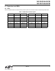
Figure 2. Si536x TQFP Block Diagram
5.3. Si536x Input and Output Clocks
The Si536x has four differential inputs that are ac terminated to 50 Ω and then ac coupled to the part. Single ended
operation can be implemented by simply not connecting to one of the two of the differential pairs.
The four clock outputs are all differential, ac coupled and configured for driving 50 Ω transmission lines. When
using single ended outputs, it is important that the unused half of the output be terminated. Given that the
Frame Sync signal can have a duty cycle that is far from 50%, the Frame Sync outputs are dc coupled. If the
Frame Sync signal is configured for CMOS output, then the two outputs are not complements of one another and
should be wired in parallel so that the output drive current is doubled. To evaluate CMOS level Frame Sync
outputs, a 0 Ω resistor should be installed at R19. Note that for the MCU controlled parts (Si5367 and Si5368), the
Frame Sync output signal format can be configured independently of the other four outputs.
Two jumpers are provided to assist in monitoring the Si536x power. When R36 is removed, J25 can be used to
measure the device current. J18 can be used at any time to monitor the supply voltage at the device.
The Si5366 and Si5368 require that an external reference clock be provided to enable the devices to operate as
narrowband jitter attenuators with loop bandwidths as low as 60 Hz. The external reference clock can be either a
crystal, a stand-alone oscillator or some other clock source. The range of acceptable reference frequencies is
described in the Any-Rate Precision Clocks Family Reference Manual (Si53xx-RM). The EVB's are shipped with a
3rd overtone 114.285 MHz crystal that is used in the majority of applications. J1 and J2 are used when the Si536x
is to be configured in narrowband mode with an external reference oscillator (i.e. without using the 114.285 MHz
crystal). When operating in wideband mode, the reference oscillator should be disabled and so that it cannot add to
the output phase noise.
The RATE pins should also be configured for the desired mode, either through DSPLLsim or using the jumper
plugs at J17 (see Table 7).
Table 2 shows how the various components should be configured for the three modes of operation:
USB
MCU
SPI bus
CPLD
ss
+3.3 V
DUT PWR
+1.8 V
Vreg
Reset
switch
LEDs
SPI bus
1.8 to 3.3 V
reg addr
Si536x
Output
SMAs
Input
SMAs
Ext RefClk
Jumper
Headers
Terminate
status signals
SPI, I
2
C signals
Control signals
CKOUT1
CKOUT2
CKOUT3
CKOUT4
FSOUT