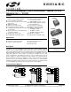
Si5351A/B/C I 2 C - P R O GRA MM A B LE A NY - F R E Q U E N C Y CMOS C L O C K G ENERATOR + VCXO Features Generates up to 8 non-integer-related frequencies from 8 kHz to 160 MHz 2 I C user definable configuration Exact frequency synthesis at each output (0 ppm error) Highly linear VCXO Optional clock input (CLKIN) Low output period jitter: 100 ps pp Configurable spread spectrum selectable at each output Operates from a low-cost, fixed frequency crystal: 25 or 27 MHz Support
Si5351A/B/C 2 Preliminary Rev. 0.
Si5351A/B/C TABLE O F C ONTENTS Section Page 1. Electrical Specifications . . . . . . . . . . . . . . . . . . . . . . . . . . . . . . . . . . . . . . . . . . . . . . . . . . .4 2. Detailed Block Diagrams . . . . . . . . . . . . . . . . . . . . . . . . . . . . . . . . . . . . . . . . . . . . . . . . . . .9 3. Functional Description . . . . . . . . . . . . . . . . . . . . . . . . . . . . . . . . . . . . . . . . . . . . . . . . . . . 11 3.1. Input Stage . . . . . . . . . . . . . . . . . . . . . . . . . . . .
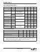
Si5351A/B/C 1. Electrical Specifications Table 1. Recommended Operating Conditions Parameter Symbol Ambient Temperature TA Core Supply Voltage VDD Output Buffer Voltage Test Condition VDDOx Min Typ Max Unit –40 25 85 °C 3.0 3.3 3.60 V 2.25 2.5 2.75 V 1.71 1.8 1.89 V 2.25 2.5 2.75 V 3.0 3.3 3.60 V Notes:All minimum and maximum specifications are guaranteed and apply across the recommended operating conditions.
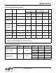
Si5351A/B/C Table 3. AC Characteristics (VDD = 2.5 V ±10%, or 3.3 V ±10%, TA = –40 to 85 °C) Parameter Symbol Test Condition Min Typ Max Unit Power-up Time TRDY From VDD = VDDmin to valid output clock, CL = 5 pF, fCLKn > 1 MHz — 1 10 ms Output Enable Time TOE From OEB pulled low to valid clock output, CL = 5 pF, fCLKn > 1 MHz — — 10 µs Output Phase Offset PSTEP — 333 — ps/step Spread Spectrum Frequency Deviation SSDEV Down spread –0.1 — –2.5 % Center spread ±0.1 — ±1.
Si5351A/B/C Table 5. Output Clock Characteristics (VDD = 2.5 V ±10%, or 3.3 V ±10%, TA = –40 to 85 °C) Parameter Symbol Test Condition Min Typ Max Units Frequency Range FCLK 0.008 — 160 MHz Load Capacitance CL — 5 15 pF Duty Cycle DC 45 50 55 % 0.5 1 1.5 ns 0.5 1 1.5 ns VDD – 0.6 — — V — — 0.
Si5351A/B/C Table 7. I2C Specifications (SCL,SDA)1 Parameter Symbol LOW Level Input Voltage VILI2C HIGH Level Input Voltage VIHI2C Hysteresis of Schmitt Trigger Inputs VHYS LOW Level Output Voltage (open drain or open collector) at 3 mA Sink Current VOLI2C2 Test Condition Standard Mode Fast Mode 100 kbps 400 kbps Unit Min Max Min Max –0.5 0.3 x VDDI2 –0.5 0.3 x VDDI2C2 V 3.63 0.7 x VDDI2C2 3.63 V — — 0.1 — V VDDI2C2 = 2.5/3.3 V 0 0.4 0 0.4 V VDDI2C2 = 1.
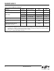
Si5351A/B/C Table 9. Absolute Maximum Ratings1 Parameter Symbol DC Supply Voltage VDD_max Test Condition Value Unit –0.5 to 3.8 V VIN_CLKIN CLKIN, SCL, SDA –0.5 to 3.8 V VIN_VC VC –0.5 to (VDD+0.3) V VIN_XA/B Pins XA, XB –0.5 to 1.3 V V TJ –55 to 150 °C Soldering Temperature (Pb-free profile)2 TPEAK 260 °C Soldering Temperature Time at TPEAK (Pb-free profile)2 TP 20–40 Sec Input Voltage Junction Temperature Notes: 1.
Si5351A/B/C 2.
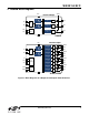
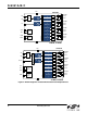
Si5351A/B/C VDD XA OSC PLL XB VCXO VC SDA SCL OEB SSEN 2 IC Interface Control Logic GND Si5351B VDDOA MultiSynth 0 R0 MultiSynth 1 R1 MultiSynth 2 R2 MultiSynth 3 R3 MultiSynth 4 R4 MultiSynth 5 R5 MultiSynth 6 R6 MultiSynth 7 R7 OSC XB PLL A PLL B CLKIN SDA SCL I2C Interface INTR OEB Control Logic CLK1 VDDOB CLK2 CLK3 VDDOC CLK4 CLK5 VDDOD CLK6 CLK7 20-QFN, 24-QSOP VDD XA CLK0 Si5351C VDDOA MultiSynth 0 R0 MultiSynth 1 R1 MultiSynth 2 R2 MultiSynth 3 R3 Mult
Si5351A/B/C 3. Functional Description The Si5351 is a versatile I2C programmable clock generator that is ideally suited for replacing crystals, crystal oscillators, VCXOs, PLLs, and buffers. A block diagram showing the general architecture of the Si5351 is shown in Figure 3. The device consists of an input stage, two synthesis stages, and an output stage. The input stage accepts an external crystal (XTAL), a clock input (CLKIN), or a control voltage input (VC) depending on the version of the device (A/B/C).
Si5351A/B/C 3.1.2. External Clock Input (CLKIN) The external clock input is used as a clock reference for the PLLs when generating synchronous clock outputs. CLKIN can accept any frequency from 10 to 100 MHz. A divider at the input stage limits the PLL input frequency to 30 MHz. 3.1.3. Voltage Control Input (VC) The VCXO architecture of the Si5350B eliminates the need for an external pullable crystal. Only a standard, lowcost, fixed-frequency (25 or 27 MHz) AT-cut crystal is required.
Si5351A/B/C 3.4. Spread Spectrum Spread spectrum can be enabled on any of the clock outputs that use PLLA as its reference. Spread spectrum is useful for reducing electromagnetic interference (EMI). Enabling spread spectrum on an output clock modulates its frequency, which effectively reduces the overall amplitude of its radiated energy. See “AN554: Si5350/51 PCB Layout Guide” for details. Note that spread spectrum is not available on clocks synchronized to PLLB or to the VCXO.
Si5351A/B/C 4. I2C Interface Many of the functions and features of the Si5351 are controlled by reading and writing to the RAM space using the I2C interface. The following is a list of the common features that are controllable through the I2C interface. A summary of register functions is shown in Section 7.
Si5351A/B/C Write Operation – Single Byte S Slv Addr [6:0] 0 A Reg Addr [7:0] A Data [7:0] A P Write Operation - Burst (Auto Address Increment) S Slv Addr [6:0] 0 A Reg Addr [7:0] A Data [7:0] A Data [7:0] A P Reg Addr +1 From slave to master From master to slave 1 – Read 0 – Write A – Acknowledge (SDA LOW) N – Not Acknowledge (SDA HIGH) S – START condition P – STOP condition Figure 9. I2C Write Operation A read operation is performed in two stages.
Si5351A/B/C 5. Configuring the Si5351 The Si5351 is a highly flexible clock generator which is entirely configurable through its I2C interface. The device’s default configuration is stored in non-volatile memory (NVM) as shown in Figure 11. The NVM is a one time programmable memory (OTP) which can store a custom user configuration at power-up. This is a useful feature for applications that need a clock present at power-up (e.g., for providing a clock to a processor).
Si5351A/B/C Disable Outputs Set CLKx_DIS high; Reg. 3 = 0xFF Powerdown all output drivers Reg. 16, 17, 18, 19, 20, 21, 22, 23 = 0x80 Set interrupt masks (see register 2 description) Register Map Use ClockBuilder Desktop v3.1 or later Write new configuration to device using the contents of the register map generated by ClockBuilder Desktop. This step also powers up the output drivers. (Registers 15-92 and 149-170) Apply PLLA and PLLB soft reset Reg.
Si5351A/B/C 5.2. Si5351 Application Examples The Si5351 is a versatile clock generator which serves a wide variety of applications. The following examples show how it can be used to replace crystals, crystal oscillators, VCXOs, and PLLs. 5.3. Replacing Crystals and Crystal Oscillators Using an inexpensive external crystal, the Si5351A can generate up to 8 different free-running clock frequencies for replacing crystals and crystal oscillators.
Si5351A/B/C 5.4. Replacing Crystals, Crystal Oscillators, and VCXOs The Si5351B combines free-running clock generation and a VCXO in a single package for cost sensitive video applications. An example is shown in Figure 14. Free-running Clocks XA OSC 27 MHz Multi Synth 0 PLL Multi Synth 1 XB Multi Synth 2 VC VCXO Multi Synth 3 Multi Synth 4 Multi Synth 5 Si5351B CLK0 125 MHz CLK1 48 MHz CLK2 28.322 MHz Ethernet PHY USB Controller HDMI Port CLK3 CLK4 74.25 MHz 74.25/1.
Si5351A/B/C 5.6. Replacing a Crystal with a Clock The Si5351 can be driven with a clock signal through the XA input pin. VIN = 1 VPP 25/27 MHz XA 0.1 µF Multi Synth 0 PLLA Multi Synth 1 OSC XB PLLB Multi Synth N Note: Float the XB input while driving the XA input with a clock Figure 16. Si5351 Driven by a Clock Signal 5.7. HCSL Compatible Outputs The Si5351 can be configured to support HCSL compatible swing when the VDDO of the output pair of interest is set to 2.5 V (i.e., VDDOA must be 2.
Si5351A/B/C 6. Design Considerations The Si5351 is a self-contained clock generator that requires very few external components. The following general guidelines are recommended to ensure optimum performance. Refer to “AN554: Si5350/51 PCB Layout Guide” for additional layout recommendations. 6.1. Power Supply Decoupling/Filtering The Si5351 has built-in power supply filtering circuitry and extensive internal Low Drop Out (LDO) voltage regulators to help minimize the number of external bypass components.
Si5351A/B/C 6.6. Trace Characteristics The Si5351A/B/C features various output current drives ranging from 2 to 8 mA (default). It is recommended to configure the trace characteristics as shown in Figure 18 when an output drive setting of 8 mA is used. ZO = 85 ohms R = 0 ohms CLK (Optional resistor for EMI management) Length = No Restrictions Figure 18. Recommended Trace Characteristics with 8 mA Drive Strength Setting Note: Jitter is only specified at 6 and 8 mA drive strength. 22 Preliminary Rev. 0.
Si5351A/B/C 7. Register Map Summary The following is a summary of the register map used to read status, control, and configure the Si5351.
Si5351A/B/C Register 7 6 5 66 4 3 2 1 67 MS3_P3[7:0] 68 R3_DIV[2:0] 69 MS3_P1[17:16] MS3_P1[15:8] 70 MS3_P1[7:0] 71 MS3_P3[19:16] 72 MS3_P2[19:16] MS3_P2[15:8] 73 MS3_P2[7:0] 74 MS4_P3[15:8] 75 MS4_P3[7:0] 76 R4_DIV[2:0] 77 MS4_P1[17:16] MS4_P1[15:8] 78 MS4_P1[7:0] 79 MS4_P3[19:16] 80 MS4_P2[19:16] MS4_P2[15:8] 81 MS4_P2[7:0] 82 MS5_P3[15:8] 83 MS5_P3[7:0] 84 R5_DIV[2:0] 85 MS5_P1[17:16] MS5_P1[15:8] 86 MS5_P1[7:0] 87 MS5_P3[19:16] MS5_P2[19:16] 88 MS5_P2
Si5351A/B/C 8. Register Descriptions Register 0. Device Status Bit D7 D6 D5 D4 Name SYS_INIT LOL_B LOL_A LOS Type R R R R D3 D2 D1 D0 REVID[1:0] R R R Reset value = 0000 0000 Bit 7 Name Function SYS_INIT System Initialization Status. During power up the device copies the content of the NVM into RAM and performs a system initialization. The device is not operational until initialization is complete.
Si5351A/B/C Register 1. Interrupt Status Sticky Bit Name Type D7 D6 D5 D4 D3 D2 D1 D0 R/W R/W R/W R/W SYS_INIT_STKY LOL_B_STKY LOL_A_STKY LOS_STKY R/W R/W R/W R/W Reset value = 0000 0000 Bit 7 Name Function SYS_INIT_STKY System Calibration Status Sticky Bit. The SYS_INIT_STKY bit is triggered when the SYS_INIT bit (register 0, bit 7) is triggered high. It remains high until cleared. Writing a 0 to this register bit will cause it to clear.
Si5351A/B/C Register 2. Interrupt Status Mask Bit Name Type D7 D6 D5 D4 D3 D2 D1 D0 R/W R/W R/W R/W SYS_INIT_MASK LOL_B_MASK LOL_A_MASK LOS_MASK R/W R/W R/W R/W Reset value = 0000 0000 Bit 7 Name Function SYS_INIT_MASK System Initialization Status Mask. Use this mask bit to prevent the INTR pin (Si5351C only) from going low when SYS_INIT is asserted. 0: Do not mask the SYS_INIT interrupt. 1: Mask the SYS_INIT interrupt. 6 LOL_B_MASK PLLB Loss Of Lock Status Mask.
Si5351A/B/C Register 3. Output Enable Control Bit Name Type D7 D6 D5 D4 D3 D2 D1 D0 CLK7_OEB CLK6_OEB CLK5_OEB CLK4_OEB CLK3_OEB CLK2_OEB CLK1_OEB CLK0_OEB R/W R/W R/W R/W R/W R/W R/W R/W D2 D1 D0 Reset value = 0000 0000 Bit 7:0 Name Function CLKx_OEB Output Disable for CLKx. Where x = 0, 1, 2, 3, 4, 5, 6, 7 0: Enable CLKx output. 1: Disable CLKx output. Register 9.
Si5351A/B/C Register 15. PLL Input Source Bit D7 D6 D5 D4 D2 D1 D0 R/W R/W PLLB_SRC PLLA_SRC Name Type D3 R/W R/W R/W R/W R/W R/W Reset value = 0000 0000 Bit Name Function 7:4 Reserved 3 PLLB_SRC Input Source Select for PLLB. 0: Select the XTAL input as the reference clock for PLLB (Si5351A/C only). 1: Select the CLKIN input as the reference clock for PLLB (Si5351C only). 2 PLLA_SRC Input Source Select for PLLA. 0: Select the XTAL input as the reference clock for PLLA.
Si5351A/B/C Register 16. CLK0 Control Bit D7 D6 D5 D4 D3 D2 D1 D0 Name CLK0_PDN MS0_INT MS0_SRC CLK0_INV CLK0_SRC[1:0] CLK0_IDRV[1:0] Type R/W R/W R/W R/W R/W R/W Reset value = 0000 0000 Bit Name 7 CLK0_PDN Function Clock 0 Power Down. This bit allows powering down the CLK0 output driver to conserve power when the output is unused. 0: CLK0 is powered up. 1: CLK0 is powered down. 6 MS0_INT MultiSynth 0 Integer Mode.
Si5351A/B/C Register 17. CLK1 Control Bit D7 D6 D5 D4 D3 D2 D1 D0 Name CLK1_PDN MS1_INT MS1_SRC CLK1_INV CLK1_SRC[1:0] CLK1_IDRV[1:0] Type R/W R/W R/W R/W R/W R/W Reset value = 0000 0000 Bit Name 7 CLK1_PDN Function Clock 1 Power Down. This bit allows powering down the CLK1 output driver to conserve power when the output is unused. 0: CLK1 is powered up. 1: CLK1 is powered down. 6 MS1_INT MultiSynth 1 Integer Mode.
Si5351A/B/C Register 18. CLK2 Control Bit D7 D6 D5 D4 D3 D2 D1 D0 Name CLK2_PDN MS2_INT MS2_SRC CLK2_INV CLK2_SRC[1:0] CLK2_IDRV[1:0] Type R/W R/W R/W R/W R/W R/W Reset value = 0000 0000 Bit Name 7 CLK2_PDN Function Clock 2 Power Down. This bit allows powering down the CLK2 output driver to conserve power when the output is unused. 0: CLK2 is powered up. 1: CLK2 is powered down. 6 MS2_INT MultiSynth 2 Integer Mode.
Si5351A/B/C Register 19. CLK3 Control Bit D7 D6 D5 D4 D3 D2 D1 D0 Name CLK3_PDN MS3_INT MS3_SRC CLK3_INV CLK3_SRC[1:0] CLK3_IDRV[1:0] Type R/W R/W R/W R/W R/W R/W Reset value = 0000 0000 Bit Name 7 CLK3_PDN Function Clock 3 Power Down. This bit allows powering down the CLK3 output driver to conserve power when the output is unused. 0: CLK3 is powered up. 1: CLK3 is powered down. 6 MS3_INT MultiSynth 3 Integer Mode.
Si5351A/B/C Register 20. CLK4 Control Bit D7 D6 D5 D4 D3 D2 D1 D0 Name CLK4_PDN MS4_INT MS4_SRC CLK4_INV CLK4_SRC[1:0] CLK4_IDRV[1:0] Type R/W R/W R/W R/W R/W R/W Reset value = 0000 0000 Bit Name 7 CLK4_PDN Function Clock 4 Power Down. This bit allows powering down the CLK4 output driver to conserve power when the output is unused. 0: CLK4 is powered up. 1: CLK4 is powered down. 6 MS4_INT MultiSynth 4 Integer Mode.
Si5351A/B/C Register 21. CLK5 Control Bit D7 D6 D5 D4 D3 D2 D1 D0 Name CLK5_PDN MS5_INT MS5_SRC CLK5_INV CLK5_SRC[1:0] CLK5_IDRV[1:0] Type R/W R/W R/W R/W R/W R/W Reset value = 0000 0000 Bit Name 7 CLK5_PDN Function Clock 5 Power Down. This bit allows powering down the CLK5 output driver to conserve power when the output is unused. 0: CLK4 is powered up. 1: CLK4 is powered down. 6 MS5_INT MultiSynth 5 Integer Mode.
Si5351A/B/C Register 22. CLK6 Control Bit D7 D6 D5 D4 D3 D2 D1 D0 Name CLK6_PDN FBA_INT MS6_SRC CLK6_INV CLK6_SRC[1:0] CLK6_IDRV[1:0] Type R/W R/W R/W R/W R/W R/W Reset value = 0000 0000 Bit Name 7 CLK6_PDN Function Clock 7 Power Down. This bit allows powering down the CLK6 output driver to conserve power when the output is unused. 0: CLK6 is powered up. 1: CLK6 is powered down. 6 FBA_INT FBA MultiSynth Integer Mode.
Si5351A/B/C Register 23. CLK7 Control Bit D7 D6 D5 D4 D3 D2 D1 D0 Name CLK7_PDN FBB_INT MS7_SRC CLK7_INV CLK7_SRC[1:0] CLK7_IDRV[1:0] Type R/W R/W R/W R/W R/W R/W Reset value = 0000 0000 Bit Name 7 CLK7_PDN Function Clock 7 Power Down. This bit allows powering down the CLK7 output driver to conserve power when the output is unused. 0: CLK7 is powered up. 1: CLK7 is powered down. 6 FBB_INT FBB MultiSynth Integer Mode.
Si5351A/B/C Register 24. CLK3–0 Disable State Bit D7 D6 D5 D4 D3 D2 D1 D0 Name CLK3_DIS_STATE CLK2_DIS_STATE CLK1_DIS_STATE CLK0_DIS_STATE Type R/W R/W R/W R/W Reset value = 0000 0000 Bit Name Function 7:0 CLKx_DIS_STATE Clock x Disable State. Where x = 0, 1, 2, 3. These 2 bits determine the state of the CLKx output when disabled. Individual output clocks can be disabled using register Output Enable Control located at address 3. Outputs are also disabled using the OEB pin.
Si5351A/B/C Register 42. Multisynth0 Parameters Bit D7 D6 D5 D4 D3 Name MS0_P3[15:8] Type R/W D2 D1 D0 Reset value = xxxx xxxx Bit 7:0 Name MS0_P3[15:8] Function Multisynth0 Parameter 3. This 20-bit number is an encoded representation of the denominator for the fractional part of the MultiSynth0 Divider. Register 43. Multisynth0 Parameters Bit D7 D6 D5 D4 D3 Name MS0_P3[7:0] Type R/W D2 D1 D0 Reset value = xxxx xxxx Bit Name 7:0 MS0_P3[7:0] Function Multisynth0 Parameter 3.
Si5351A/B/C Register 44. Multisynth0 Parameters Bit D7 D6 Name Type D5 D4 D3 D2 R0_DIV[2:0] R/W D1 D0 MS0_P1[17:16] R/W R/W R/W R/W Reset value = xxxx xxxx Bit Name 7 Unused 6:4 R0_DIV[2:0] Function R0 Output Divider. 000b: Divide by 1 001b: Divide by 2 010b: Divide by 4 011b: Divide by 8 100b: Divide by 16 101b: Divide by 32 110b: Divide by 64 111b: Divide by 128 3:2 Reserved 1:0 MS0_P1[17:16] Multisynth0 Parameter 1.
Si5351A/B/C Register 46. Multisynth0 Parameters Bit D7 D6 D5 D4 D3 Name MS0_P1[7:0] Type R/W D2 D1 D0 Reset value = xxxx xxxx Bit Name 7:0 MS0_P1[7:0] Function Multisynth0 Parameter 1. This 18-bit number is an encoded representation of the integer part of the MultiSynth1 divider. Register 47. Multisynth0 Parameters Bit D7 D6 D5 D4 D3 D2 D1 Name MS0_P3[19:16] MS0_P2[19:16] Type R/W R/W D0 Reset value = xxxx xxxx Bit Name 7:4 MS0_P3[19:16] Function Multisynth0 Parameter 3.
Si5351A/B/C Register 49. Multisynth0 Parameters Bit D7 D6 D5 D4 D3 Name MS0_P2[7:0] Type R/W D2 D1 D0 Reset value = xxxx xxxx Bit Name 7:0 MS0_P2[7:0] Function Multisynth0 Parameter 2. This 20-bit number is an encoded representation of the numerator for the fractional part of the MultiSynth1 Divider. Register 50. Multisynth1 Parameters Bit D7 D6 D5 D4 D3 Name MS1_P3[15:8] Type R/W D2 D1 D0 Reset value = xxxx xxxx Bit Name 7:0 MS1_P3[15:8] Function Multisynth1 Parameter 3.
Si5351A/B/C Register 52. Multisynth1 Parameters Bit D7 D6 D4 D3 D2 R1_DIV[2:0] Name Type D5 R/W D1 D0 MS1_P1[17:16] R/W R/W R/W R/W Reset value = xxxx xxxx Bit Name 7 Unused 6:4 R1_DIV[2:0] Function R1 Output Divider. 000b: Divide by 1 001b: Divide by 2 010b: Divide by 4 011b: Divide by 8 100b: Divide by 16 101b: Divide by 32 110b: Divide by 64 111b: Divide by 128 3:2 Reserved 1:0 MS1_P1[17:16] Multisynth1 Parameter 1.
Si5351A/B/C Register 54. Multisynth1 Parameters Bit D7 D6 D5 D4 D3 Name MS1_P1[7:0] Type R/W D2 D1 D0 Reset value = xxxx xxxx Bit Name 7:0 MS1_P1[7:0] Function Multisynth1 Parameter 1. This 18-bit number is an encoded representation of the integer part of the MultiSynth1 divider. Register 55. Multisynth1 Parameters Bit D7 D6 D5 D4 D3 D2 D1 Name MS1_P3[19:16] MS1_P2[19:16] Type R/W R/W D0 Reset value = xxxx xxxx Bit Name 7:4 MS1_P3[19:16] Function Multisynth1 Parameter 3.
Si5351A/B/C Register 57. Multisynth1 Parameters Bit D7 D6 D5 D4 D3 Name MS1_P2[7:0] Type R/W D2 D1 D0 Reset value = xxxx xxxx Bit Name 7:0 MS1_P2[7:0] Function Multisynth1 Parameter 2. This 20-bit number is an encoded representation of the numerator for the fractional part of the MultiSynth1 divider. Register 58. Multisynth1 Parameters Bit D7 D6 D5 D4 D3 Name MS1_P3[15:8] Type R/W D2 D1 D0 Reset value = xxxx xxxx Bit Name 7:0 MS1_P3[15:8] Function Multisynth1 Parameter 3.
Si5351A/B/C Register 60. Multisynth2 Parameters Bit D7 D6 Name Type D5 D4 D3 D2 R2_DIV[2:0] R/W D1 D0 MS2_P1[17:16] R/W R/W R/W R/W Reset value = xxxx xxxx Bit Name 7 Unused 6:4 R2_DIV[2:0] Function R2 Output Divider. 000b: Divide by 1 001b: Divide by 2 010b: Divide by 4 011b: Divide by 8 100b: Divide by 16 101b: Divide by 32 110b: Divide by 64 111b: Divide by 128 3:2 Reserved 1:0 MS2_P1[17:16] Multisynth2 Parameter 1.
Si5351A/B/C Register 62. Multisynth2 Parameters Bit D7 D6 D5 D4 D3 Name MS2_P1[7:0] Type R/W D2 D1 D0 Reset value = xxxx xxxx Bit Name 7:0 MS2_P1[7:0] Function Multisynth2 Parameter 1. This 18-bit number is an encoded representation of the integer part of the Multisynth2 divider. Register 63. Multisynth2 Parameters Bit D7 D6 D5 D4 D3 D2 D1 Name MS2_P3[19:16] MS2_P2[19:16] Type R/W R/W D0 Reset value = xxxx xxxx Bit Name 7:4 MS2_P3[19:16] Function Multisynth2 Parameter 3.
Si5351A/B/C Register 65. Multisynth2 Parameters Bit D7 D6 D5 D4 D3 Name MS2_P2[7:0] Type R/W D2 D1 D0 Reset value = xxxx xxxx Bit Name 7:0 MS2_P2[7:0] Function Multisynth2 Parameter 2. This 20-bit number is an encoded representation of the numerator for the fractional part of the Multisynth2 divider. Register 66. Multisynth3 Parameters Bit D7 D6 D5 D4 D3 Name MS3_P3[15:8] Type R/W D2 D1 D0 Reset value = xxxx xxxx Bit Name 7:0 MS3_P3[15:8] Function Multisynth3 Parameter 3.
Si5351A/B/C Register 68. Multisynth3 Parameters Bit D7 D6 Name Type D5 D4 D3 D2 R3_DIV[2:0] R/W D1 D0 MS3_P1[17:16] R/W R/W R/W R/W Reset value = xxxx xxxx Bit Name 7 Unused 6:4 R3_DIV[2:0] Function R3 Output Divider. 000b: Divide by 1 001b: Divide by 2 010b: Divide by 4 011b: Divide by 8 100b: Divide by 16 101b: Divide by 32 110b: Divide by 64 111b: Divide by 128 3:2 Reserved 1:0 MS3_P1[17:16] Multisynth3 Parameter 1.
Si5351A/B/C Register 70. Multisynth3 Parameters Bit D7 D6 D5 D4 D3 Name MS3_P1[7:0] Type R/W D2 D1 D0 Reset value = xxxx xxxx Bit Name 7:0 MS3_P1[7:0] Function Multisynth3 Parameter 1. This 18-bit number is an encoded representation of the integer part of the Multisynth3 divider. Register 71. Multisynth3 Parameters Bit D7 D6 D5 D4 D3 D2 D1 Name MS3_P3[19:16] MS3_P2[19:16] Type R/W R/W D0 Reset value = xxxx xxxx Bit Name 7:4 MS3_P3[19:16] Function Multisynth3 Parameter 3.
Si5351A/B/C Register 73. Multisynth3 Parameters Bit D7 D6 D5 D4 D3 Name MS3_P2[7:0] Type R/W D2 D1 D0 Reset value = xxxx xxxx Bit Name 7:0 MS3_P2[7:0] Function Multisynth3 Parameter 2. This 20-bit number is an encoded representation of the numerator for the fractional part of the Multisynth3 divider. Register 74. Multisynth4 Parameters Bit D7 D6 D5 D4 D3 Name MS4_P3[15:8] Type R/W D2 D1 D0 Reset value = xxxx xxxx Bit Name 7:0 MS4_P3[15:8] Function Multisynth4 Parameter 3.
Si5351A/B/C Register 76. Multisynth4 Parameters Bit D7 D6 Name Type D5 D4 D3 D2 R4_DIV[2:0] R/W D1 D0 MS4_P1[17:16] R/W R/W R/W R/W Reset value = xxxx xxxx Bit Name 7 Unused 6:4 R4_DIV[2:0] Function R4 Output Divider. 000b: Divide by 1 001b: Divide by 2 010b: Divide by 4 011b: Divide by 8 100b: Divide by 16 101b: Divide by 32 110b: Divide by 64 111b: Divide by 128 3:2 Reserved 1:0 MS4_P1[17:16] Multisynth4 Parameter 1.
Si5351A/B/C Register 78. Multisynth4 Parameters Bit D7 D6 D5 D4 D3 Name MS4_P1[7:0] Type R/W D2 D1 D0 Reset value = xxxx xxxx Bit Name 7:0 MS4_P1[7:0] Function Multisynth4 Parameter 1. This 18-bit number is an encoded representation of the integer part of the Multisynth4 divider. Register 79. Multisynth4 Parameters Bit D7 D6 D5 D4 D3 D2 D1 Name MS4_P3[19:16] MS4_P2[19:16] Type R/W R/W D0 Reset value = xxxx xxxx Bit Name 7:4 MS4_P3[19:16] Function Multisynth4 Parameter 3.
Si5351A/B/C Register 81. Multisynth4 Parameters Bit D7 D6 D5 D4 D3 Name MS4_P2[7:0] Type R/W D2 D1 D0 Reset value = xxxx xxxx Bit Name 7:0 MS4_P2[7:0] Function Multisynth4 Parameter 2. This 20-bit number is an encoded representation of the numerator for the fractional part of the Multisynth4 divider. Register 82. Multisynth5 Parameters Bit D7 D6 D5 D4 D3 Name MS5_P3[15:8] Type R/W D2 D1 D0 Reset value = xxxx xxxx Bit Name 7:0 MS5_P3[15:8] Function Multisynth5 Parameter 3.
Si5351A/B/C Register 84. Multisynth5 Parameters Bit D7 D6 Name Type D5 D4 D3 D2 R5_DIV[2:0] R/W D1 D0 MS5_P1[17:16] R/W R/W R/W R/W Reset value = xxxx xxxx Bit Name 7 Unused 6:4 R5_DIV[2:0] Function R5 Output Divider. 000b: Divide by 1 001b: Divide by 2 010b: Divide by 4 011b: Divide by 8 100b: Divide by 16 101b: Divide by 32 110b: Divide by 64 111b: Divide by 128 3:2 Reserved 1:0 MS5_P1[17:16] Multisynth5 Parameter 1.
Si5351A/B/C Register 86. Multisynth5 Parameters Bit D7 D6 D5 D4 D3 Name MS5_P1[7:0] Type R/W D2 D1 D0 Reset value = xxxx xxxx Bit Name 7:0 MS5_P1[7:0] Function Multisynth5 Parameter 1. This 18-bit number is an encoded representation of the integer part of the Multisynth5 divider. Register 87. Multisynth5 Parameters Bit D7 D6 D5 D4 D3 D2 D1 Name MS5_P3[19:16] MS5_P2[19:16] Type R/W R/W D0 Reset value = xxxx xxxx Bit Name 7:4 MS5_P3[19:16] Function Multisynth5 Parameter 3.
Si5351A/B/C Register 89. Multisynth5 Parameters Bit D7 D6 D5 D4 D3 Name MS5_P2[7:0] Type R/W D2 D1 D0 Reset value = xxxx xxxx Bit Name 7:0 MS5_P2[7:0] Function Multisynth5 Parameter 2. This 20-bit number is an encoded representation of the numerator for the fractional part of the Multisynth5 Divider. Register 90. Multisynth6 Parameters Bit D7 D6 D5 D4 D3 Name MS6_P1[7:0] Type R/W D2 D1 D0 Reset value = xxxx xxxx Bit Name 7:0 MS6_P1[7:0] Function Multisynth6 Parameter 1.
Si5351A/B/C Register 92. Clock 6 and 7 Output Divider Bit D7 Name Type D6 D5 D4 D3 R7_DIV[2:0] R/W R/W Name 7 Reserved 6:4 R7_DIV[2:0] R/W Function Leave as default. R7 Output Divider. 000b: Divide by 1 001b: Divide by 2 010b: Divide by 4 011b: Divide by 8 100b: Divide by 16 101b: Divide by 32 110b: Divide by 64 111b: Divide by 128 3 Reserved 1:0 R6_DIV[2:0] Leave as default. R6 Output Divider.
Si5351A/B/C Register 165. CLK0 Initial Phase Offset Bit D7 D6 D5 D4 D2 D1 D0 R/W R/W R/W CLK0_PHOFF[6:0] Name Type D3 R/W R/W R/W R/W R/W Reset value = 0000 0000 Bit Name 7 Reserved 6:0 Function Only write 0 to this bit. CLK0_PHOFF[6:0] Clock 0 Initial Phase Offset. CLK0_PHOFF[6:0] is an unsigned integer with one LSB equivalent to a time delay of Tvco/4, where Tvco is the period of the VCO/PLL associated with this output. Register 166.
Si5351A/B/C Register 168. CLK3 Initial Phase Offset Bit D7 D6 D5 D4 D2 D1 D0 R/W R/W R/W CLK3_PHOFF[6:0] Name Type D3 R/W R/W R/W R/W R/W Reset value = 0000 0000 Bit Name 7 Reserved 6:0 Function Only write 0 to this bit. CLK3_PHOFF[6:0] Clock 3 Initial Phase Offset. CLK3_PHOFF[6:0] is an unsigned integer with one LSB equivalent to a time delay of Tvco/4, where Tvco is the period of the VCO/PLL associated with this output. Register 169.
Si5351A/B/C Register 177. PLL Reset Bit D7 Name PLLB_RST Type R/W D6 D5 D4 D3 D2 D1 D0 R/W R/W R/W R/W R/W PLLA_RST R/W R/W Reset value = 0000 0000 Bit 7 Name Function PLLB_RST PLLB_Reset. Writing a 1 to this bit will reset PLLB. This is a self clearing bit (Si5351A/C only). 6 5 Reserved Leave as default. PLLA_RST PLLA_Reset. Writing a 1 to this bit will reset PLLA. This is a self clearing bit. 4:0 Reserved Leave as default. Register 183.
Si5351A/B/C 9.
Si5351A/B/C 10.
Si5351A/B/C 11.
Si5351A/B/C 12. Si5351A Pin Descriptions (10-Pin MSOP) Si5351A 10-MSOP Top View VDD 1 10 CLK0 XA 2 9 CLK1 XB 3 8 GND SCL 4 7 VDDO SDA 5 6 CLK2 Table 13. Si5351A 10-MSOP Pin Descriptions Pin Name Pin Number Pin Type* Function 10-MSOP XA 2 I Input pin for external crystal. XB 3 I Input pin for external crystal. CLK0 10 O Output clock 0. CLK1 9 O Output clock 1. CLK2 6 O Output clock 2. SCL 4 I Serial clock input for the I2C bus.
Si5351A/B/C 13. Ordering Information Si5351X A XX *Note: The 10-MSOP is only available in the Si5351A variant. GT = 10-MSOP* GM = 20-QFN GU = 24-QSOP A = Product Revision A A = Crystal In B = Crystal In + VCXO C = Crystal In + CLKIN Figure 19. Device Part Numbers An evaluation kit containing ClockBuilder Desktop software and hardware enable easy evaluatin of the Si5351A/B/C. The orderable part numbers for the evaluation kits are provided in Figure 20.
Si5351A/B/C 14. Package Outline (24-Pin QSOP) Table 14. 24-QSOP Package Dimensions Dimension Min Nom Max A — — 1.75 A1 0.10 — 0.25 b 0.19 — 0.30 c 0.15 — 0.25 D 8.55 8.65 8.75 E E1 6.00 BSC 3.81 e L 3.99 0.635 BSC 0.40 L2 q 3.90 — 1.27 0.25 BSC 0 — aaa 0.10 bbb 0.17 ccc 0.10 8 Notes: 1. All dimensions shown are in millimeters (mm) unless otherwise noted. 2. Dimensioning and Tolerancing per ANSI Y14.5M-1994. 3.
Si5351A/B/C 15. Package Outline (20-Pin QFN) Table 15. Package Dimensions Dimension A A1 b D D2 e E E2 L aaa bbb ccc ddd eee Min 0.80 0.00 0.18 2.65 2.65 0.30 Nom 0.85 0.02 0.25 4.00 BSC 2.70 0.50 BSC 4.00 BSC 2.70 0.40 Max 0.90 0.05 0.30 2.75 2.75 0.50 0.10 0.10 0.08 0.10 0.10 Notes: 1. All dimensions shown are in millimeters (mm) unless otherwise noted. 2. Dimensioning and Tolerancing per ANSI Y14.5M-1994. 3. This drawing conforms to the JEDEC Outline MO-220, variation VGGD-8. 4.
Si5351A/B/C 16. Package Outline (10-Pin MSOP) Table 16. 24-QSOP Package Dimensions Dimension A A1 A2 b c D E E1 e L L2 q aaa bbb ccc ddd Min — 0.00 0.75 0.17 0.08 0.40 0 — — — — Nom — — 0.85 — — 3.00 BSC 4.90 BSC 3.00 BSC 0.50 BSC 0.60 0.25 BSC — — — — — Max 1.10 0.15 0.95 0.33 0.23 0.80 8 0.20 0.25 0.10 0.08 Notes: 1. All dimensions shown are in millimeters (mm) unless otherwise noted. 2. Dimensioning and Tolerancing per ANSI Y14.5M-1994. 3.
Si5351A/B/C DOCUMENT CHANGE LIST Revision 0.1 to Revision 0.9 Updated max output frequency. Updated kV values in Table 3 on page 5. Updated "3.4. Spread Spectrum" on page 13. Added "5.1. Writing a Custom Configuration to RAM" on page 16. Added "5.7. HCSL Compatible Outputs" on page 20. Added "6.6. Trace Characteristics" on page 22. Updated "8. Register Descriptions" on page 25. Added register descriptions. Revision 0.9 to Revision 0.95 Added 1.8 V VDDO support.
Si5351A/B/C NOTES: Preliminary Rev. 0.
Si5351A/B/C CONTACT INFORMATION Silicon Laboratories Inc. 400 West Cesar Chavez Austin, TX 78701 Tel: 1+(512) 416-8500 Fax: 1+(512) 416-9669 Toll Free: 1+(877) 444-3032 Please visit the Silicon Labs Technical Support web page: https://www.silabs.com/support/pages/contacttechnicalsupport.aspx and register to submit a technical support request. The information in this document is believed to be accurate in all respects at the time of publication but is subject to change without notice.