
- Silicon Laboratories, Inc. Radio User Manual


Si4734/35-B20
Rev. 1.0 9
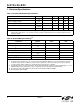
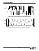
Figure 4. 3-Wire Control Interface Write Timing Parameters
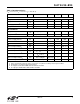
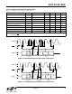
Figure 5. 3-Wire Control Interface Read Timing Parameters
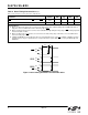
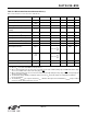
Table 6. 3-Wire Control Interface Characteristics
(V
DD
= 2.7 to 5.5 V, V
IO
= 1.5 to 3.6 V, T
A
= –20 to 85 °C)
Parameter Symbol Test Condition Min Typ Max Unit
SCLK Frequency f
CLK
0—2.5MHz
SCLK High Time t
HIGH
25 — — ns
SCLK Low Time t
LOW
25 — — ns
SDIO Input, SEN
to SCLK↑ Setup t
S
20 — — ns
SDIO Input to SCLK↑ Hold t
HSDIO
10 — — ns
SEN
Input to SCLK↓ Hold t
HSEN
10 — — ns
SCLK↑ to SDIO Output Valid t
CDV
Read 2 — 25 ns
SCLK↑ to SDIO Output High Z t
CDZ
Read 2 — 25 ns
SCLK, SEN
, SDIO, Rise/Fall time t
R
, t
F
— — 10 ns
Note: When selecting 3-wire mode, the user must ensure that a rising edge of SCLK does not occur within 300 ns before the
rising edge of RST
.
SCLK
70%
30%
SEN
70%
30%
SDIO
A7 A0
70%
30%
t
S
t
S
t
HSDIO
t
HSEN
A6-A5,
R/W,
A4-A1
Address In Data In
D15 D14-D1 D0
t
HIGH
t
LOW
t
R
t
F
½ Cycle Bus
Turnaround
SCLK
70%
30%
SEN
70%
30%
SDIO
70%
30%
t
HSDIO
t
CDV
t
CDZ
Address In Data Out
A7 A0
A6-A5,
R/W,
A4-A1
D15 D14-D1 D0
t
S
t
S
t
HSEN