
- Silicon Laboratories, Inc. Radio User Manual


Si4734/35-B20
Rev. 1.0 5
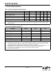
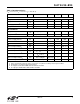
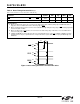
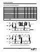
Table 3. DC Characteristics
(V
DD
= 2.7 to 5.5 V, V
IO
= 1.5 to 3.6 V, T
A
= –20 to 85 °C)
Parameter Symbol Test Condition Min Typ Max Unit
FM Mode
Supply Current I
FM
—19.222mA
Supply Current
1
I
FM
Low SNR level — 19.8 23 mA
RDS Supply Current
2
I
FM
—19.923mA
Supply Current
2
I
FMD
Digital Output Mode — 18.0 20.5 mA
AM/SW/LW Mode
Supply Current I
AM
Analog Output Mode — 17.3 20.5 mA
Supply Current
2
I
AMD
Digital Output Mode — 15.5 20.5 mA
Supplies and Interface
Interface Supply Current I
IO
—320600µA
V
DD
Powerdown Current I
DDPD
—1020 µA
V
IO
Powerdown Current I
IOPD
SCLK, RCLK inactive — 1 10 µA
High Level Input Voltage
3
V
IH
0.7 x V
IO
—V
IO
+0.3 V
Low Level Input Voltage
3
V
IL
–0.3 — 0.3 x V
IO
V
High Level Input Current
3
I
IH
V
IN
= V
IO
= 3.6 V –10 — 10 µA
Low Level Input Current
3
I
IL
V
IN
=0V,
V
IO
=3.6V
–10 — 10 µA
High Level Output Voltage
4
V
OH
I
OUT
= 500 µA 0.8 x V
IO
——V
Low Level Output Voltage
4
V
OL
I
OUT
= –500 µA — — 0.2 x V
IO
V
Notes:
1. LNA is automatically switched to higher current mode for optimum sensitivity in weak signal conditions.
2. Specifications are guaranteed by characterization.
3. For input pins SCLK, SEN, SDIO, RST, RCLK, DCLK, and DFS.
4. For output pins SDIO, DOUT, GPO1, GPO2, and GPO3.