
User Guide

C8051T620/2-DK
8 Rev. 0.4
7. Development Boards
The C8051T620/2 Development Kit includes a motherboard that interfaces to various daughter boards. The
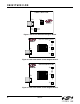
C8051T62x Emulation Daughter Board contains a C8051F34A device to be used for preliminary software
development. The C8051T620 Socket Daughter Board and C8051T622 Socket Daughter Board allow
programming and evaluation of the actual C8051T62x devices. Numerous input/output (I/O) connections are
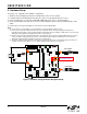
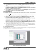
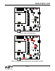
provided on the motherboard to facilitate prototyping. Figure 3 shows the C8051T62x Motherboard and indicates
locations for various I/O connectors. Figure 4 shows the factory default shorting block positions. Figures 5, 6, and 7
show the available C8051T62x daughter boards. Figures 8, 9, 10, and 11 show the available C8051T32x daughter
boards.
P1, P2 Daughter board connection
P3 Power connector that accepts input from 7.5 to 15 V dc unregulated power adapter
P4 USB connector for UART to USB communications interface
P5 USB Debug interface connector
J1 Analog I/O terminal block
J2 Port 0 header
J3 Port 1 header
J4 Port 2 header
J5 Port 3 header with access to VDD and GND
J6 Power supply selection header (See "7.3. Power Supply Headers (J6 and J7)" on page 14)
J7 Power supply enable header that connects power source selected on J6 to the board's main
power supply net
J8 Communications interface control signal header
J9 Connects port pins to the switches labeled “SW1” and “SW2”
J10 Connects port pins to the LEDs labeled “LED1” and “LED2”
J11 Communications interface data signal header
J12 Connects potentiometer to the port pin, P2.5
J13 Additional connections to ground
J14 Connects an external VREF from J1 to P0.7
J15 VPP supply connection used when programming EPROM devices