
- Silicon Laboratories, Inc. Computer Drive - USB Flash Drive User Manual


C8051F340/1/2/3/4/5/6/7
60 Rev. 0.5
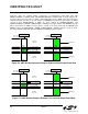
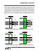
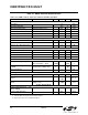
Figure 7.1. Comparator Functional Block Diagram
Comparator outputs can be polled in software, used as an interrupt source, and/or routed to a Port pin.
When routed to a Port pin, Comparator outputs are available asynchronous or synchronous to the system
clock; the asynchronous output is available even in STOP mode (with no system clock active). When dis
-
abled, the Comparator output (if assigned to a Port I/O pin via the Crossbar) defaults to the logic low state,
and supply current falls to less than 100
nA. See Section “15.1. Priority Crossbar Decoder” on
page 149 for details on configuring Comparator outputs via the digital Crossbar. Comparator inputs can be
externally driven from –0.25 V to (V
DD
) + 0.25 V without damage or upset. The complete Comparator elec-
trical specifications are given in Table 7.1.
Comparator response time may be configured in software via the CPTnMD registers (see SFR Definition
7.3 and SFR Definition 7.6). Selecting a longer response time reduces the Comparator supply current. See
Table 7.1 for complete timing and supply current specifications.
VDD
CPTnCN
Reset Decision Tree
(Comprator 0 Only)
+
-
Crossbar
Interrupt
Logic
Q
Q
SET
CLR
D
Q
Q
SET
CLR
D
(SYNCHRONIZER)
GND
CPn +
CPn -
CPnEN
CPnOUT
CPnRIF
CPnFIF
CPnHYP1
CPnHYP0
CPnHYN1
CPnHYN0
CPTnMD
CPnRIE
CPnFIE
CPnMD1
CPnMD0
CPn
CPnA
CPn
Rising-edge
CPn
Falling-edge
CPn
Interrupt
CPnRIE
CPnFIE
CPTnMX
CMXnN1
CMXnN0
CMXnP1
CMXnP0
CMXnN2
CMXnP2
Port I/O connection options vary with
package (32-pin or 48-pin)