
Daim Ntawv Qhia Tus Neeg Siv


3.3 Breakout Pads
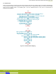
Most pins of the EFR32 are routed from the radio board to breakout pads at the top and bottom edges of the Wireless STK Mainboard.
A 2.54 mm pitch pin header can be soldered on for easy access to the pins. The figure below shows you how the pins of the EFR32
maps to the pin numbers printed on the breakout pads. To see the available functions on each, refer to the data sheet for
EFR32FG1P133F256GM48.
GND
VMCU
P23 / NC
P21 / NC
P19 / NC
P17 / NC
GND
P15 / NC
P13 / PC11 / EXP16 / I2C_SDA
P11 / PA1 / EXP14 / VCOM_RX
P9 / PA0 / EXP12 / VCOM_TX
P7 / PC9 / EXP10
P5 / PC8 / EXP8 / FLASH_SCLK / DISP_SCLK
P3 / PC7 / EXP6 / FLASH_MISO
P1 / PC6 / EXP4 / FLASH_MOSI / DISP_SI
VRF
GND
VMCU
PTI_SYNC / PB13 / P22
PTI_DATA / PB12 / P20
PTI_CLK / PB11 / P18
VCOM_ENABLE / PA5 / P16
GND
FLASH_SCS / PA4 / P14
I2C_SCL / EXP15 / PC10 / P12
DBG_TDI / EXP13 / PF3 / P10
LED0 / EXP11 / PF4 / P8
BTN1 / EXP9 / PF7 / P6
BTN0 / EXP7 / PF6 / P4
VCOM_RTS / EXP5 / PA3 / P2
VCOM_CTS / EXP3 / PA2 / P0
VRF
J101
GNDGND
5V5V
NCNC
P45 / NCNC / P44
P43 / NCNC / P42
P41 / NCNC / P40
3V33V3
P39 / NCNC / P38
P37 / PD15 / DISP_ENABLE / SENSOR_ENABLENC / P36
P35 / PD15 / DISP_ENABLE / SENSOR_ENABLENC / P34
P33 / PD14 / DISP_SCSLED1 / PF5 / P32
P31 / PD13 / DISP_EXTCOMINNC / P30
P29 / NCDBG_TDO_SWO / PF2 / P28
P27 / NCDBG_TMS_SWDIO / PF1 / P26
P25 / NCDBG_TCK_SWCLK / PF0 / P24
GNDGND
J102
Figure 3.2. Breakout Pad Pin Mapping
UG185: EFR32FG1 2400/169 MHz Dual Band Radio Board User's Guide
Connectors
silabs.com | Building a more connected world. Rev. 1.1 | 8
Downloaded from Arrow.com.Downloaded from Arrow.com.Downloaded from Arrow.com.Downloaded from Arrow.com.Downloaded from Arrow.com.Downloaded from Arrow.com.Downloaded from Arrow.com.Downloaded from Arrow.com.