
Daim Ntawv Qhia Tus Neeg Siv

C8051F50x/51x
Rev. 0.2 9
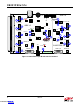
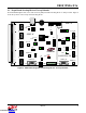
5.4. Switches and LEDs
Two push-button switches are provided on the target board for each MCU. Switch RESET_A is connected to the
/RST pin of the C8051F500. Switch RESET_B is connected to the /RST pin of the C8051F502. Pressing
RESET_A puts the C8051F500 device into its hardware-reset state, and similarly for RESET_B and the
C8051F502 MCU. Switches P1.4_A and P1.4_B are connected to the MCU’s general purpose I/O (GPIO) pins
through headers. Pressing either one of these switches generates a logic low signal on the port pin. Remove the
shorting block from the header to disconnect these switches from the port pins. See Table 2 for the port pins and
headers corresponding to each switch.
Four LEDs are provided on the target board to serve as indicators. The red LED labeled PWR indicates presence
of power to the target board. The second red LED labeled COMM indicates if the CP2102 USB-to-UART bridge
(P5) is recognized by the PC. The green LED labeled with port pin name P1.3_A is connected to the C8051F500’s
(Side A) GPIO pin P1.3 through the header J19. Remove the shorting block from the header to disconnect the LED
from the port pin. Similarly, the green LED named P1.3_B is connected to the C8051F502 (Side B) through the J11
header. See Table 2 for the port pins and headers corresponding to each LED.
5.5. Target Board Debug Interfaces (P2 and P3)
The
debug
connectors P2 (DEBUG_A) and P3 (DEBUG_B) provide access to the
debug
(C2) pins of the
C8051F500 and C8051F502. The
debug
connectors are used to connect the Serial Adapter or the USB Debug
Adapter to the target board for in-circuit debugging and Flash programming. Table 3 shows the
DEBUG
pin
definitions.
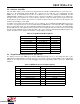
Table 2. Target Board I/O Descriptions
Description I/O Header(s)
RESET_A Reset (Side A) none
RESET_B Reset (Side B) none
P1.4_A Switch P1.4 (Side A) J191–2]
P1.4_B Switch P1.4 (Side B) J11[1–2]
P1.3_A LED P1.3 (Side A) J19[3–4]
P1.3_B LED P1.3 (Side B) J11[3–4]
Red LED (PWR) Power none
Red LED (COMM) COMM Active none
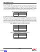
Table 3. DEBUG Connector Pin Descriptions
Side A - C8051F500 Side B - C8051F502
Pin # Description Pin # Description
1 Not Connected 1 Not Connected
2, 3, 9 GND (Ground) 2, 3, 9 GND (Ground)
4 C2D_A 4 P3.0_C2D_B
5 /RST (Reset) 5 /RST_B (Reset)
6 Not Connected 6 P3.0_B
7 /RST/C2CK_A 7 /RST/C2CK_B
8 Not Connected 8 Not Connected
10 USB Power (+5VDC from P2) 10 Not Connected
Downloaded from Arrow.com.Downloaded from Arrow.com.Downloaded from Arrow.com.Downloaded from Arrow.com.Downloaded from Arrow.com.Downloaded from Arrow.com.Downloaded from Arrow.com.Downloaded from Arrow.com.Downloaded from Arrow.com.