
User`s manual


57
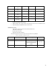
Appendix D Key West Jumpers (listed by Function)
Following is a detailed description of the jumper locations on the Key West PCB. The
jumpers are listed by function.
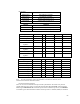
Audio/Analog
JP10 Hitachi AFE Adapter (from 465)
JP25 Speaker (miniature connector -- 2 pins) SH7729 AN7/PLT7
JP29 ADC/DAC pins (AN4 to AN7)
JP43 AUD Connector (10 pins)
AutoPC
J12 AutoPC Connector (120 pins)
JP36 AutoPC Interrupt Connector (10 pin DIP)
JP31 AutoPC Interrupt Enable
In = Enable interrupts
Out = Disable
JP39 AutoPC Power Selection ???? Remove jumper for CompactPCI ????
1-2 = 3.3 volts
2-3 = 5 volts
ATX Power Supply
JP1 ATX Power Connector
JP11 ATX Enable Power
In = Enable
Out = Disable
Big Endian / Little Endian Select
R123 0 ohm resistor/jumper for Big Endian mode
open for Little Endian mode
(7709A/7729 MD5 signal) (bottom side of PCB)
Clocks
JP5 1-2 66 MHz System clock from oscillator
Pin 1 = 66 MHz oscillator output
Pin 2 = Input for external 66 Mhz clock (for debug)
Pin 3 = Gnd
JP6 1-2 33 MHz PCI clock from oscillator
Pin 1 = 33 MHz oscillator output
Pin 2 = Input for external 33 Mhz clock (for debug)
Pin 3 = Gnd
JP8 System Clock Frequency Select
In = 33 MHz
*Out = 66 MHz