
User`s manual


53
Appendix C SH7709A/7729 Registers
The following is a detailed description of the SH3 registers used to initialize the processor at
power-up/reset time.
Bus Control Register 1 (BCR1)
Bus control register 1 (BCR1) is a 16-bit read/write register that sets the functions and bus
cycle state for each area. It is initialized to H'0000 by a power-on reset, but is not initialized
by a manual reset or by standby mode. Do not access external memory outside area 0 until
BCR1 register initialization is complete.
Bus Control Register 2 (BCR2)
The bus control register 2 (BCR2) is a 16-bit read/write register that selects the bus-size width
of each area. It is initialized to H'3FFC by a power-on reset, but is not initialized by a manual
reset or by standby mode. Do not access external memory outside area 0 until BCR2 register
initialization is complete.
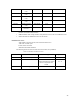
Bus control register 1 BCR1 H'FFFFFF60 0x0008
bit15: Pin A25 to A0 not Pulled-Up ( 0 )
bit14: Pin D31 to D0 not Pulled-Up ( 0 )
bit13: Hi-Z Memory Control ( 0 )
bit12: High-Z Control ( 0 )
bit11: Endian Flag ( x )
bit10-9: Area 0 normal ROM ( 0 0 )
bit8: Area 5 normal Memory ( 0 )
bit7: Area 5 normal Memory ( 0 )
bit6-5: Area 6 normal memory ( 0 0 )
bit4: Area 2 normal, Area 3 SDRAM Memory ( 0 )
bit3-2: Area 2 normal, Area 3 SDRAM Memory ( 1 0 )
bit1: Area 5 normal memory ( 0 )
bit0: Area 6 normal memory ( 0 )
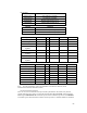
Bus control register 2 BCR2 H'FFFFFF62 0x3ff0
bit15-14: Reserved: read as 0. ( 0 0 )
bit13-12: Area 6 32-bit Bus Size ( 1 1 )
bit11-10: Area 5 32-bit Bus Size ( 1 1 )
bit9-8: Area 4 32-bit Bus Size ( 1 1 )
bit7-6: Area 3 32-bit Bus Size ( 1 1 )
bit5-4: Area 2 32-bit Bus Size ( 1 1 )
bit3-0: Reserved: read as 0. ( 0000)