
User`s manual


35
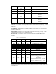
PCMCIAEN: A “1” indicates that the PCMCIA decode is enabled for CS5 & CS6 address space.
A “0” indicates that the PCI aperture decode is enabled for CS5 and CS6 and PCMCIA is not
supported.
LED0: A “1” will turn on the endplate LED used to indicate power-up condition. A “0” will turn
off that LED. This bit should power up in a “1” state. This bit is not available on a Rev 4 board.
SYSCLKSEL: A “1” indicates that we are running at full system bus speed, which in the typical
case is 66MHz. A “0” indicates that we are running at ½ system bus clock speed.
PCICLKSEL: A “1” indicates that we are running at full system PCI bus speed, which in the
typical case is 33MHz. A “0” indicates that we are running at ½ PCI bus clock speed.
HD_CLKDIV2: A “1” indicates that we are running the MQ200 and the HD64465 at ½ the clock
speed of the rest of the system bus. A “0” indicates the hardware is running at the full system bus
speed.
SW1 Register
Base Address: 0x11FF B000
Data Assignments (RO = Read-Only, RW = Read-Write):
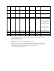
D07 D06 D05 D04 D03 D02 D01 D00
N/A N/A N/A N/A MISCSW FLASH
PROT#
DEBUG
SER#
BOOT
PROM#
RO RO RO RO RO RO RO RO
X X X X 0 X X X
These bits output the value of the HARP designated Switch 1 (S1).
MISCSW: Used for general purpose SW control. Undefined at the moment.
FLASHPROT#: When “0” indicates that the FLASH can not be written to. A “1” indicates the
FLASH can be written to.
DEBUGSER#: A “0” indicates that debug will be performed over the debug serial port. A “1”
indicates that debug is done over the debug ethernet port.
BOOTPROM#: A “0” indicates that the system booted from the BOOT PROM versus the
FLASH. A “1” indicates that the system booted from the FLASH.