
User`s manual


34
See the HP HDSP-2534 device specification for further details of this register space. All functional
aspects of this display are supported.
Special notes:
The Display is based on a byte address boundary but is in a 32 bit SH3 address space. The
processor will always try to do 32 bit write but only D[7:0] will actually be written.
The display D[7:0] is mapped to the bus D[7:0].
Physical address A[4:0] is mapped to device address A[4:0]. FL# of the device is mapped to
physical address A5.
Ethernet Device (SMSC LAN91C100FD & PHY LAN83C180)
Base Address: 0x11FE 0000
This device is mapped into a 32-bit SH3 data segment and all accesses are forced to a DWORD
boundary.
See the SMSC LAN91C100FD document for specific decoding. Note that the Frame buffer
memory (128KB), the PHY chip and the Ethernet EEPROM are all accessible via the register
mapping of the LAN91C100FD.
CPLD Registers
External Bus/Board ID Register
Base Address: 0x11FF D000
Data Assignments (RO = Read-Only, RW = Read-Write):
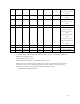
D07 D06 D05 D04 D03 D02 D01 D00
N/A N/A N/A EXT65BUS EXT64BUS BD_ID2 BD_ID1 BD_ID0
RO RO RO RO RO RO RO RO
X X X 1 1 X X X
EXT65BUS: A “1” indicates that we are driving a HD64465 chip on the daughter board. A “0”
indicates that we are driving a HD64465 on the main board.
EXT64BUS: A “1” indicates that we are driving a MQ200 chip on the daughter board. A “0”
indicates that we are driving a MQ200 on the main board.
BD_ID[2:0]: These bits represent different versions of Hitachi daughter boards. At present there is
no pull-up on these pins, so there is no guarantee of what state these pins will be if no external
board is present. We should be able to test to see if an external board is present by reading this
location, then writing the complementary value and then reading back the value. If no external
board is present, we should be able to read back the complementary value.
Clock Select/LED0/PCMCIAEN Register
Base Address: 0x11FF C000
Data Assignments (RO = Read-Only, RW = Read-Write):
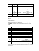
D07 D06 D05 D04 D03 D02 D01 D00
N/A PCMCIA
EN
LED0 N/A N/A SYSCLK
SEL
PCICLK
SEL
HD_CLK
DIV2
RO RO RW RO RO RO RO RO
X 0 X X X X X X