
User`s manual


32
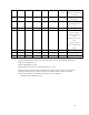
0 0x0000 0000 0x03FF FFFF 000 64MB CS0 8 bit
32 bit
Boot ROM (512k x 8) or
Flash (1M x 32 bit) with boot
from Flash
1 0x0400 0000 0x07FF FFFF 001 64MB None Internal 7709A/7729
peripherals
2 0x0800 0000 0x0BFF FFFF 010 64MB CS2 32 bit PCI Aperture
Flash with boot from Boot
ROM
3 0x0C00 0000 0x0FFF FFFF 011 64MB CS3 32 bit SDRAM
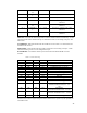
4 0x1000 0000 0x13FF FFFF 100 64MB CS4 32 bit HD64465 decode: 32 bit I/O;
Local USC registers;
Diagnostic 8 digit Alpha
display
Ethernet registers and frame
buffer
CPLD option register
V3 PCI Configuration Ports
MQ200
5 0x1400 0000 0x17FF FFFF 101 64MB CS5 32 bit PCI Aperture 1/PCMCIA 1
6 0x1800 0000 0x1BFF FFFF 110 64MB CS6 32 bit PCI Aperture 2/PCMCIA 0
7 0x1C00 0000 0x1FFF FFFF 111 64MB Reserved by Hitachi
* All data widths except Area 0 are set by internal registers. Area 0 is set by Mode pins MD3 and
MD4, and is configured by S1-1.
Ignored Address Bits: A31-A29
Shadow Offset to all addresses = 0x20000000*n where n=1 to 6
Address space Area 5 and 6 need special explanation. In both cases the address area supports two
mutually exclusive functions, either a PCI aperture or PCMCIA sockets. Jumper (J35) selects
whether the PCI aperture or the PCMCIA socket is selected for both areas.
HD64465 Memory Mapping, Area 4