
User`s manual

21
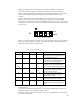
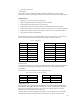
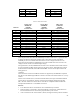
Table 2: Debug Serial Port Pin-out
Pin Name Pin Name
1 DBG_CD 6 DBG_DSR
2 DBG_RX 7 DBG_RTS
3 DBG_TX 8 DBG_CTS
4 DBG_DTR 9 DBG_RI
5 GND
This serial port (DBG_RX, DBG_TX) supports a serial data format of 8data, 1 stop and no
parity.
The output signals DBG_DTR and DBG_RTS are directly controllable via register bits. The
input signals, DBG_CD, DBG_DSR, DBG_RI, and DBG_CTS are visible as register bits.
Compact PCI Interface
The Compact PCI interface is implemented using the V3 Semiconductor V320 Bridge Chip. It
supports both master and slave modes.
CompactPCI connects to the back-plane using CPCI connectors J1 and J2 (which map to the
board connectors J11 and J7, respectively).
The CompactPCI system slot supports clock generation and arbitration. It also supports seven
REQ/GRANT pairs and seven clock sets.
Key West complies with CompactPCI PCIMG 2.0 Revision 2.1, which is an extension of PCI
specification version 2.1 and meets all PCI timing requirements for 33Mhz operation. It also
meets the requirements for a universal 3.3V/5V card.
Note: Normally the PCI interface uses memory areas 5 and 6, which provides a 128 Mbyte
memory space. Jumper J35 must be installed in order for PCI to use these memory areas.
PCMCIA also uses these memory spaces. If J35 is removed, PCMCIA uses areas 5 and 6 and
PCI is either not used or uses a much smaller memory space within Area 2.
CompactPCI Extensions
Signals ENUM#, FAIL#, DEG#, CLK5 and CLK6 are supported.
An interrupt will be generated when ENUM# is asserted.
The power supply signal FAIL# will generate a reset.
The power supply signal DEG# will interrupt the CPU in order to prepare for loss of power.
Clocks
There is a 33-MHz external crystal for the CPU which, when coupled with the
SH7709A/7729’s on-chip PLLs and clock divide circuitry, determines the speed of operation.
Setting the SH7709A/7729 mode pins determines CPU clock speed, bus clock speed, and
peripheral speed.
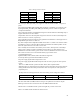
The Key West board as shipped has the clock mode setting switch configured to Mode 7.
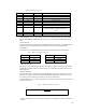
Clock Mode (MD2-0) CPU Clock CPU Bus Clock CPU Peripheral Clock
7 2x (133 MHz) 1x (66 MHz) 0.5x (33 MHz)
The main clock CKIO (66 MHz) from the CPU goes to a QS5V993 clock driver chip for
buffering. This clock driver drives the clock to the SDRAM and PCI blocks.
The RTC has a 32.768-kHz external crystal. This signal only connects to the CPU.
There is a 33-MHz external oscillator for the PCI clocks.