US7729/09A Hardware Architecture Reference Platform User’s Manual US7729-HCB1/10/11 & US7709A-HCB1/10/11 US7729-HRP10A & US7709A-HRP10A US7729-HRP11A & US7709A-HRP11A Version A.2 0850082-01 Hitachi Semiconductor (America), Inc.
Notice When using this document, keep the following in mind: 1. This document may, wholly or partially, be subject to change without notice. 2. All rights are reserved: No one is permitted to reproduce or duplicate, in any form, the whole or part of this document without Hitachi’s permission. 3. Hitachi will not be held responsible for any damage to the user that may result from accidents or any other reasons during operation of the user’s unit according to this document. 4.
Contents Section 1 Overview....................................................................................................................... 4 1.1 Introduction ................................................................................................................................4 1.2 Key West Base Board Features .................................................................................................5 1.3 Tahoe Daughter Board Features..............................................
Bus Control Register 1 (BCR1) ..........................................................................................................53 Bus Control Register 2 (BCR2) ..........................................................................................................53 Wait State Control Register 1 (WCR1) .............................................................................................54 Wait State Control Register 2 (WCR2) ................................................................
Read Me First If you do nothing else please review sections 2 and 3 before you start. This will reduce the initial startup problems that may occur. This document, as well as the hardware, is constantly being improved. Check with your technical support person periodically for available updates. A simple diagnostic monitor program, primarily written in C language and referred to as CMON, is available “as is” and at no charge after completing and returning a release form.
Section 1 Overview 1.1 Introduction The Hitachi SuperH tm microprocessor-based Hardware Architecture Reference Platform (HARP) consists of a printed circuit board (PCB) or board set, schematics, sample software device driver source code, CPLD code, gerber files, bill of materials, and documentation.
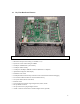
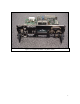
1.2 Key West Base Board Features Figure 1.1 SH7709A/7729 Base Board (Key West) • SH7709A/7729 processor running at 133 MHz (3.3 V) • System bus: 32 bits wide running at 66 MHz • 64 Mbytes of SDRAM for system memory • 32 Mbytes of flash memory • 10 Mbps and 100 Mbps 100BASE-T Ethernet (IEEE 802.
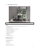
1.3 Tahoe Daughter Board Features Figure 1.2 Tahoe I/O Board HD64465 • PCMCIA interface that supports PCMCIA Rev. 2.1/JEIDA version 4.2 (2 slots) • PS/2 keyboard interface • PS/2 mouse interface • IrDA (SIR – 115.
Figure 1.
Section 2 Quick Start Guide (WinCE) This section describes the following for the SH7709A/7729 HARP: • The hardware and software requirements. • Connections between a host system and the Key West. • Downloading and running a binary image file. 2.1 System Requirements 2.1.1 Host PC Hardware and Software Requirements The user supplies a host system with the following requirements: • Hardware CPU Pentium 133 MHz or greater recommended. Memory 32MB minimum, 64 MB or greater recommended.
2.1.3 Shipped with SH7709A/7729 HARP • SH7709A/7729 base board (Key West) with face plate • System I/O daughter board (Tahoe) with face plate • Null modem serial cable • Ethernet cable • 25-pin parallel CEPC cable • ATX power supply with AC cord 2.1.
* For reference, if the user would like to boot into the WinCE OS installed in FLASH, switch S1 would be set to: OFF OFF OFF OFF 2.2 Harp Connections 2.2.1 Key West Connections 1. 2. Plug in the ATX 20-pin block power terminal to J1. Connect the serial cable from DB9 front panel connector labeled “Dbg Mfg” (J9) of the Key West board to the COM port of the host PC. 2.2.2 Tahoe Connections 1. 2. 3. 4. 5. 2.3 Plug the Tahoe 140-pin connector into the Key West 140-pin connector using “spacer board”.
5. 6. • Data bits: 8 • Parity: None • Stop bits: 1 • Flow control: None File->Save. Save these settings so that you don’t have to enter them the next time. Select “Disconnect” and “Connect” on the menu bar to force Hyperterm to use the new settings. 2.4.2 CESH (Windows CE Parallel Port Download Tool) 1. Install the Windows CE Toolkit. Enable the parallel port download option during the installation..
4. The command prompt shell will appear on the display monitor. 5. Typing dir will display a list of files and folders from Windows CE. 2.
13
Section 3 Quick Start Guide (VxWorks) The following information gives guidelines and suggestions for the setup of the SH7751 HARP when using the Wind River Tornado tools. The Wind River Tornado User’s Guide was used as a guide for some of the explanation and can be referenced for a more complete guide for the installation. 3.1 Installing Tornado 2 on a Windows Host PC There are a number of ways to set up Tornado 2 with the different platforms. This section will discuss the Windows environment.
3.2 1. 2. 3. 4. 5. 6. 3.3 Download BSP from Platform Support Site Using a standard web browser, view the following page: http://ftp.hsa.hitachi.com/netshare/capp01/ There, you will find links to the BSP files. These will be labeled “Tornado 2.0” or “T2.” They are ZIP files and are named in this manner: aspen_t2.zip; bigsur_t2.zip; keywest_t2.zip Download the keywest_t2.zip file.
3.4 1. 2. 3. 4. 5. Build VxWorks and Boot ROM Images Make sure the Tornado Registry is running. You should see its icon in the Windows tray on the taskbar. If not, start it manually from the Start→ →Programs→ →Tornado2→ →Registry shortcut. Start Tornado 2 from the start menu at Start→ →Programs→ →Tornado2→ →Tornado The “Create Project in New/Existing Workspace” dialog window should appear upon startup. If it does not appear, select “New Project” from the “File” menu.
3.5 Downloading “bootrom.hex” Image to the Target There are several methods available to download images to the target. We will use DMON’s “LE” command in conjunction with a TFTP server. Tftpd32 is a freeware TFTP server and is included in the support CD-ROM. It is also available for download on the Platform Support web page at http://ftp.hsa.hitachi.com/netshare/capp01/ as well as other locations on the Internet. Simply extract the ZIP file to a known location. Setup TFTP Server 1.
3.6 1. 2. 3. 4. 5. 6. 3.7 1. 2. 3. 4. 5. 6. Setup FTP Server →Tornado2 menu. Start the FTP server from the Start→ →Programs→ Select “Users/rights…” from the “Security” menu to open the “User / Rights Security Dialog” dialog. Click the “New User…” button. In the “User Name:” field, enter the same user name as in the config.h file from Section 2.2.3. Click the “OK” button when done. Enter a new password and verify it. This should be the same as the password in the config.h file from Section 2.2.3.
Section 4 Hardware Description Functional Description CPU The Key West may be configured with either a Hitachi SH7709A or SH7729 SH3 processor. The processor internal speed runs at 133MHz and the bus speed at 66MHz.
Pushing this button has the exact same effect as an assertion of PRST# on the CPCI bus. The system is forced into a hard-reset state whenever this button is pushed or PRST# is asserted. Releasing this button asserts PRST# which resets the HARP performs a cold reboot. All PCI reset requirements on RST# are satisfied when the PRST# signal is asserted. Switches There are two sets of DIP (dual in-line parallel) switches on Key West. Each set of DIP switches contains four switches.
Table 2: Debug Serial Port Pin-out Pin 1 2 3 4 5 Name DBG_CD DBG_RX DBG_TX DBG_DTR GND Pin 6 7 8 9 Name DBG_DSR DBG_RTS DBG_CTS DBG_RI This serial port (DBG_RX, DBG_TX) supports a serial data format of 8data, 1 stop and no parity. The output signals DBG_DTR and DBG_RTS are directly controllable via register bits. The input signals, DBG_CD, DBG_DSR, DBG_RI, and DBG_CTS are visible as register bits.
Bus Speed Frequency SDRAM 66 MHz V3-PCI Bridge 66 MHz SMSC Ethernet 66 MHz I/O Expansion 66 MHz Timers The SH7709A/7729 and 64465 chips provide five hardware timers to support Windows CE and other operating system. Under Windows CE two of these timers are assigned for kernel tasks, while the other three are available for user tasks. The Timer 1 on the SH7709A/7729 is assigned to periodically interrupt the CPU.
• False start bit detection VGA Graphics The graphics controller supports the MediaQ MQ-200 companion chip. The controller provides up to 1280 x 768 (along with many other variations) along with LCD display support. MQ-200 features: • Support for 1,2,4,15 and 16 bits per pixel (bpp). • Built-in 16Mb frame buffer for the MQ-200 video controller. • Triple 256x8 color lookup table for 1,2,4 and 8 bpp.
configuration a special parallel port cable must be used. This cable can be obtained from Redmond Cable Corp., in Redmond, WA, PN MIC-64355913 (10 ft.), described as “CE/PE Parallel Cable, DB25M to DB25M.” Table 5: Parallel Port Pin-out Pin 1 2 3 4 5 6 7 8 9 10 11 12 13 Name NSTB PPD0 PPD1 PPD2 PPD3 PPD4 PPD5 PPD6 PPD7 NACK BUSY PE SEL Pin 14 15 16 17 18 19 20 21 22 23 24 25 Name NAFD NERROR NINIT NSELIN GND GND GND GND GND GND GND GND IrDA Serial Interface The IrDA 1.
Table 6: IrDA connector Pin-out Pin 1 2 3 4 5 6 7 8 Name TX SEL1/ID1 GND VCC SEL2/ID2 ID3 IRRX2 RX1 9 10 NC NC Direction I I/O O O I/O I/O O O Function Transmit data I/O Pin for identification Ground +5V or +3.3V I/O Pin for mode select and identification. I/O Pin for identification Receive data from FIR receiver. Receive data from SIR if (SEL2 is low), or from demodulated 38KHz IR if SEL2 is high.
Table 8 HARP LCD Header Signal Definitions Name DF ENABKL ENAVDD ENAVEE P0-23 FRAME LOAD XLEFT XRIGHT YLEFT YRIGHT CP V12V V5V V3V VSENSE Function The DF signal is used on some LCD panels for internal biasing. It is a clocking signal that changes state at the beginning of each new frame while the FRAME signal is active. During all even numbered frames it will be a '1' and during odd numbered frames it will be a '0'.
43 45 47 49 P18 GND P20 P22 44 46 48 50 P19 P21 P23 GND Table 10: LCD Data Format Data Pin P0 P1 P2 P3 P4 P5 P6 P7 P8 P9 P10 P11 P12 P13 P14 P15 Citizen Color K6488L-FF 640x480 scan-line start UD7 – Upper Scan Red 0 UD6 – Upper Scan Green 0 UD5 – Upper Scan Blue 0 UD4 – Upper Scan Red 1 LD7 – Lower Scan Red 0 LD6 – Lower Scan Green 0 LD5 – Lower Scan Blue 0 LD4 – Lower Scan Red 1 UD3 – Upper Scan Green 1 UD2 – Upper Scan Blue 1 UD1 – Upper Scan Red 2 UD0 – Upper Scan Green 2 LD3 – Lower Scan Green 1 L
• Area 5 is allocated to PC Card Channel 1 (PCC1) and supports both memory and I/O interfaces. The ability to switch between Attribute memory or a Common memory, and I/O space is determined by the memory addressed by the CPU.. Note that there is an overlap of memory space for the PCI apertures and the PCMCIA socket. Via a two jumpers on the board, the user can select a PCI or PCMCIA aperture for address Areas 5 or 6. Jumper J35 must be removed from the Key West board in order to use the PCMCIA sockets.
Microsoft has a reference platform that is used for running Windows CE inside an automobile called Auto PC. It consists of a CPU and a support card attached to a PCI bus. A HARP Board may electrically connect to the Auto PC platform by adding an additional Molex connector (part number 52584-1209) to the CompactPCI bus. This connector is placed on the underside of the PCB and runs parallel to the board just in front of the CompactPCI connectors.
Signal Name Definition CS3 Chip select for the 64 Mbytes of SDRAM RAS3L/PTJ0 RAS for lower 32 Mbytes SDRAM RAS3U/PTE2 RAS for upper 32 Mbytes SDRAM CASLL/CAS/PTJ2 CAS for lower 32 Mbytes SDRAM CASLH/CAS/PTJ3 CAS for upper 32 Mbytes SDRAM CKE/PTK5 CKE for all SDRAM R/W Read/write for all SDRAM WE[0:3] Upper and lower DQMs for SDRAM CKIO Clock for all SDRAM Note: The 100 MHz SDRAM parts will be used.
Section 5 Programmer’s Guide Memory Map The SH7729 Key West Demonstration Platform is a stand-alone computing system. The SH3 MCU supports up to seven external chip select spaces: Boot Flash (EPROM), SDRAM, PCI, Ethernet, Parallel Port, PCMCIA, and daughter card interface. The flash-memory resource can be erased and reprogrammed in 64 Kbytes blocks and provides protection for bootstrap program storage. The SH-3 processor has a fixed partition of address space.
0 0x0000 0000 0x03FF FFFF 000 64MB CS0 1 0x0400 0000 0x07FF FFFF 001 64MB None 2 0x0800 0000 0x0BFF FFFF 010 64MB CS2 8 bit Boot ROM (512k x 8) or 32 bit Flash (1M x 32 bit) with boot from Flash Internal 7709A/7729 peripherals 32 bit PCI Aperture Flash with boot from Boot ROM 3 0x0C00 0000 0x0FFF FFFF 011 64MB CS3 32 bit SDRAM 4 0x1000 0000 0x13FF FFFF 100 64MB CS4 32 bit HD64465 decode: 32 bit I/O; Local USC registers; Diagnostic 8 digit Alpha display Ethernet registe
Table 13: HD64465 Address Mapping 0x100000000x10000FFF 0x100010000x10001FFF 0x100020000x10002FFF Standby & System Register Reserved PCMCIA Register 0x100030000x10003FFF AFE I/F Register 0x100040000x10004FFF GPIO Register 0x100050000x10005FFF INTC Register 0x100060000x10006FFF Timer Register 0x100070000x10007FFF IrDA Register 0x100080000x10008FFF UART Register 0x100090000x10009FFF Embeded SRAM 0x1000A0000x1000AFFF Parallel Port Register 0x1000B0000x1000BFFF USB Host Register 0x1000C0000x
See the HP HDSP-2534 device specification for further details of this register space. All functional aspects of this display are supported. Special notes: The Display is based on a byte address boundary but is in a 32 bit SH3 address space. The processor will always try to do 32 bit write but only D[7:0] will actually be written. The display D[7:0] is mapped to the bus D[7:0]. Physical address A[4:0] is mapped to device address A[4:0]. FL# of the device is mapped to physical address A5.
PCMCIAEN: A “1” indicates that the PCMCIA decode is enabled for CS5 & CS6 address space. A “0” indicates that the PCI aperture decode is enabled for CS5 and CS6 and PCMCIA is not supported. LED0: A “1” will turn on the endplate LED used to indicate power-up condition. A “0” will turn off that LED. This bit should power up in a “1” state. This bit is not available on a Rev 4 board. SYSCLKSEL: A “1” indicates that we are running at full system bus speed, which in the typical case is 66MHz.
Debug Register Base Address: 0x11FF A000 Data Assignments (RO = Read-Only, RW = Read-Write): D07 D06 D05 D04 D03 D02 D01 D00 N/A DEBUG6 DEBUG5 DEBUG4 DEBUG3 DEBUG2 DEBUG1 DEBUG0 RW RW RW RW RW RW RW RW X X X X X X X X This port is available for debug purposes to support any boot time self-test.
Table 14: MQ-200 Address Mapping 0x1200 00000x12FF FFFF 16MB Frame Buffer 0x1300 00000x13DF FFFF Reserved 14MB 0x13E0 00000x13FF FFFF 64464 Register Space 2MB See the MQ200 specification for further definition of these address spaces.
S1-2 DEBUSERIA L# 7709A/7729 PTG1; Rev 4 Bd. or less only S1-3 FLASHPROT # 7709A/7729 PTG2; Rev 4 Bd. or less only S1-4 MISCSW 7709A/7729 PTG3; Rev 4 Bd. or less only S1-1 BOOTPROM# U6 – CPLD See 0 above. Applies to Rev 5 Bd. and above S1-2 DEBUSERIA L# U6 – CPLD See 0 above. Applies to Rev 5 Bd. and above S1-3 FLASHPROT # U6 – CPLD See 0 above. Applies to Rev 5 Bd. and above S1-4 MISCSW U6 – CPLD See 0 above. Applies to Rev 5 Bd.
Table 18: SDRAM 64MB tests Test Number Data Width Test/Data Written 1 32 bit Write Background of 0xFFFFFFFF and then walk through and read background, write foreground of 0x00000000, then read foreground 2 32 bit Write Background of 0x00000000 and then walk through and read background, write foreground of 0xFFFFFFFF, then read foreground 3 32 bit Write Background of 0xAAAAAAAA and then walk through and read background, write foreground of 0x55555555, then read foreground 4 32 bit Write Background of 0x55555
Compact PCI Interface The Compact PCI bus interface supports four standard bus interrupts A, B, C and D. Additionally we need to support two legacy ISA interrupts: INTP, and INTS. We need to support hot swap through a final interrupt, ENUM, which indications a board has been inserted or removed. See Interrupt section 0 below, for further interrupt assignment information.
Timers . The timer resources are in the 7709A/7729 and the HD64465 companion chip.
PP_BUSY HD64465 BUSY PP_PE HD64465 PE PP_SLCT HD64465 SLCT PP_IPD[0..7] HD64465 PPD[0..7] PS/2 Mouse Port The PS/2 mouse support is used in the HD64465. Table 27: PS/2 Mouse Port Assignments Signal Source I/O Port Mouse Data HD64465 MSDAT Mouse Clock HD64465 MSCK Notes LCD Panel Support Table 28: LCD Panel Resource Assignment Signal Source I/O Port FP_ENVDD MQ-200 ENVDD FP_ENCTL MQ-200 ENCTL FP_ENVEE MQ-200 ENVEE FPDATA[0..23] MQ-200 FD[0..
PC0WP HD64465 PCC0WP#/IOIS16# PC0RDY HD64465 PCC0RDY/IREQ0# PC0BVD1 HD64465 PCC0BVD1/STSC HG0# PC0BVD2 HD64465 PCC0BVD2/SPKR0 PC0CD1 HD64465 PCC0CD1# PC0CD2 HD64465 PCC0CD2# PC0VS1 HD64465 PCC0VS1# PC0VS2 HD64465 PCC0VS2# PC0REG HD64465 PCC0REG# PC0SEL0 HD64465 VCC0SEL0/CLOC K PC0SEL1 HD64465 VCC0SEL1/DATA PC0VPP1 HD64465 VCC0VPP1/LATC H HD64465 VCC0VPP0 Not used HD64465 P8OLE Not used PC0D[0..15] HD64465 PCC0D[0..15] PC0A[0..25] HD64465 PCC0A[0..
USB These signals connect to the two stacked USB connectors on the Tahoe board. Table 30: USB Resource Assignment Signal Source I/O Port USBPEN# HD64465 USBPEN# USBOVR# HD64465 USBOVR# USBD1P HD64465 USBD1P USBD1M HD64465 USBD1N USBD2P HD64465 USBD2P USBD2M HD64465 USBD2N Notes AutoPC AutoPC is typically not enabled. Note that the AutoPC is in conflict with the E10 JTAG ports, so they are mutually exclusive.
Table 32: Sound System Resource Assignment Signal Source I/O Port AD_ACCLK HD64465 ACCLK AD_ACRST# HD64465 ACRST# AD_ACPD# HD64465 ACPD#/ACIRQ/PW E# AD_SIBDIN HD64465 SIBDIN AD_SIBCLK HD64465 SIBCLK AD_SIBDOUT HD64465 SIBDOUT AD_SIBSYNC HD64465 SIBSYNC Notes A/D Converters Table 33: A/D Converter Port Assignment Signal Source I/O Port AD4 7709A/7729 AN4/PTL4 AD5 7709A/7729 AN5/PLT5 AD6 7709A/7729 AN6/DA0/PLT6 Notes This port can also be used as a DA output.
SENOUT6 HD64465 PA6 R/W SENOUT7 HD64465 PA7 R/W Smart Card Interface Table 36: Smart Card Port Assignment Signal Source I/O Port SH_SCRXD 7709A/7729 RXD0/SCPT0 SH_SCTXD 7709A/7729 TXD0/SCPT0 SH_SCCLC 7709A/7729 SCK0/SCPT1 Notes 46
Four Wire Touch Screen Input Table 37: Four-Wire Touch Screen Resource Assignment Signal Source I/O Port Notes GPIO3 HD64465 PE2 Output GPIO2 HD64465 PE1 Output GPIO1 HD64465 PE0 Output TSPX HD64465 TSPX Analog Input TSMX HD64465 TSMX Analog Input TSPY HD64465 TSPY Analog Input TSMY HD64465 TSMY Analog Input Miscellaneous Resource Assignments Table 38: Miscellaneous Resource Assignments Signal Source I/O Port Notes EXP_INT 7709A/7729 PTC7/PINT7 Daughterboard, optiona
TP HD64465 PE[4..
PINT10 AutoPC Interrupt conn. AUTOINT2 Low PINT11 AutoPC Interrupt conn. AUTOINT3 Low PINT12 AutoPC Interrupt conn. AUTOINT4 Low PINT13 AutoPC Interrupt conn. AUTOINT5 Low PINT14 AutoPC Interrupt conn. AUTOINT6 Low PINT15 AutoPC Interrupt connector. AUTOINT7 Low • Hardware Initialization Requirements SDRAM address mux. timing should be setup identical on the V320 versus SH7709A/7729 • SH3 should float the SDRAM bus when not bus master HD64465 Area: Area 4 2.
RS-232 Ports SCIF Port Definition RXD1/SCPT2 DTR (software controlled) SCK1/SCPT3 CD (software controlled) RxD2/SCPT4 Receive data (console, port 1) TxD2/SCPT4 Transmit data (console, port 1) SCI Port Definition RxD0/SCPT0 Receive data (console, port 0) TxD0/SCPT0 Transmit data (console, port 0) SCIF Register Name Abbreviation R/W Initial Value Address Access Size Serial mode register 2 SCSMR2 Bit rate register 2 SCBRR2 R/W H'00 H'4000150 8 bits R/W H'FF H'4000152 8 bits Se
Appendix A Key West Bill of Material (BOM) This will is listed on the CD that can be obtained after signing the Agreement included in the Shipping box.
Appendix B Tahoe PCB Bill of Material (BOM) This is listed on the CD that can be obtained after signing the Agreement included in the Shipping box.
Appendix C SH7709A/7729 Registers The following is a detailed description of the SH3 registers used to initialize the processor at power-up/reset time. Bus Control Register 1 (BCR1) Bus control register 1 (BCR1) is a 16-bit read/write register that sets the functions and bus cycle state for each area. It is initialized to H'0000 by a power-on reset, but is not initialized by a manual reset or by standby mode. Do not access external memory outside area 0 until BCR1 register initialization is complete.
Wait State Control Register 1 (WCR1) Wait state control register 1 (WCR1) specifies the idle time between area changes and a read to a write in the same area. bit15: bit14: bit13-12: bit11-10: bit9-8: bit7-6: bit5-4: bit3-2: bit1-0: Wait state control register 1 WCR1 H'FFFFFF64 0x3cf3 WAIT Sampling at rising edge of CKIO ( 0 Reserved: read as 0.
Individual Memory Control Register (MCR) The individual memory control register (MCR) is a 16-bit read/write register that specifies RAS and CAS timing and burst control for DRAM (area 3 only), SDRAM (areas 2 and 3), specifies address multiplexing, and controls refresh. This enables direct connection of DRAM and SDRAM without external circuits. The MCR is initialized to H'0000 by power-on resets, but is not initialized by manual resets or standby mode.
Refresh Time Constant Register (RTCOR) Refresh time constant register (RTCOR) defines the period between each refresh cycle. It is calculated by getting from the SDRAM data sheet the number of refresh cycles to be completed by a certain time frame.
Appendix D Key West Jumpers (listed by Function) Following is a detailed description of the jumper locations on the Key West PCB. The jumpers are listed by function.
JP41 & JP42 Clock Skew Controls clock skew for: Sysclk, SDRAM Off-board clocks.
PCI and PCMCIA J5 & J7 & J11 CompactPCI Connectors JP7 PCI Clock Frequency Select In = 16.
Appendix E Key West Jumpers (listed by Jumper number) Following is a list of the jumper locations on the Key West PCB. The jumpers are listed in numerical order. JP1 Disable Tahoe MQ-200 JP2 System CPLD (6 pin SIP connector) JP3 N/A JP4 N/A JP5 66 MHz System clock source JP6 33 MHz PCI clock source JP7 PCI Clock Frequency (16.
J5 J6 J7 J8 J9 J10 J11 J12 CompactPCI Connector VGA Connector (15 pin female) CompactPCI Connector USB Connector (4 pins) Serial Debug (9 pin male) Expansion connector (140 pins) CompactPCI Connector AutoPC Connector (120 pins) T1 RJ45 Ethernet Connector 61
Appendix F Tahoe Daughterboard Connectors External Connectors J1 Line In J2 Mono Mic In J3 Amplified headphone out J4A PS/2 Keyboard Connector (5 pin DIN female) J4B PS/2 Mouse Connector (5 pin DIN female) J5A VGA Connector (15 pin female) J5B Product RS-232 Serial J5C Parallel Port (25 pin female0 J6A USB (lower) J6B USB (upper) J8 PCMCIA Socket (upper) J9 PCMCIA Socket (lower) 62