
Specifications

Product Technical Specification & Customer Design Guidelines
26 Proprietary and Confidential - Contents subject to change 4114634
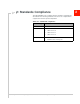
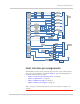
Note: The following table describes the internal structure of the module.
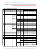
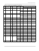
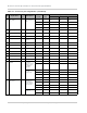
Table 3-1: Connector pin assignments
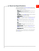
1
Pin Signal name
Pin
type
2
Description
Direction
to module
Active
state
Voltage levels (V)
Min Typ Max
1 WAKE_N OC Wake host Output Low - - 0.10
2 VCC V Power supply Input Power 3.00 3.30 3.60
3 ANT_CTRL0 /
GPIO1
- (ANT_CTRL0)
Customer-
defined external
switch control
for multiple
antennas
Output High 1.35 - 1.90
Output Low 0 - 0.45
(GPIO1)
General
purpose I/O
Input High 1.17 1.80 2.10
Input Low -0.30 0.63
Output High 1.35 1.80 1.90
Output Low 0.00 0.45
4 GND V Ground Input Power - 0 -
5 ANT_CTRL1 /
GPIO2
- (ANT_CTRL1)
Customer-
defined external
switch control
for multiple
antennas
Output High 1.35 - 1.90
Output Low 0 - 0.45
(GPIO2)
General
purpose I/O
Input High 1.17 1.80 2.10
Input Low -0.30 0.63
Output High 1.35 1.80 1.90
Output Low 0.00 0.45
6 NC - No connect - - - - -
7 NC - No connect - - - - -
8 USIM_PWR - SIM VCC supply Output Power 2.75 (3V SIM)
1.75 (1.8V SIM)
2.85 (3V SIM)
1.80 (1.8V SIM)
3.05 (3V SIM)
1.85 (1.8V SIM)
9 GND V Ground Input Power - 0 -
10 USIM_DATA - SIM IO pin Input Low -0.30 (3V SIM)
-0.30 (1.8V SIM)
- 0.70 (3V SIM)
0.63 (1.8V SIM)
High 1.85 (3V SIM)
1.17 (1.8V SIM)
2.85 (3V SIM)
1.80 (1.8V SIM)
3.15 (3V SIM)
2.10 (1.8V SIM)
Output Low 0 - 0.45
High 2.40 (3V SIM)
1.35 (1.8V SIM)
- 2.85 (3V SIM)
1.90 (1.8V SIM)