
Instruction manual

Model 5100-99-IT 4-20 mA Transmitter
Page: 8
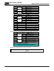
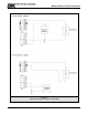
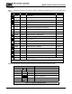
P1 PCB Label Function
1 IN + Digital Input SW +
2
Switch
IN - Digital Input SW -
3 IN + 4-20 mA Input +
4
4-20
IN - 4-20 mA Input -
5 GND Ground
6 OUT + 4-20 mA Output +
7
4-20
OUT - 4-20 mA Output -
P2 PCB Label Function
1 + RS 485 (+) (A)
2 - RS 485 (-) (B)
3
RS 485
S RS 485 shield (Isolated GND)
4 + RS 485 (+) (A)
5 - RS 485 (-) (B)
6
RS 485
S RS 485 shield (Isolated GND)
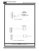
P3B PCB Label Function
1 P VDC Power
2 S Sentry Signal or Communication
3 G VDC Ground
P3A
4 P VDC Power
5 S Sentry Signal or Communication
6 G VDC Ground
P4 Connections are only available when the optional Relays are included
P4 PCB Label Function
1 N/C Low Alarm Relay NC
2 COM Low Alarm Relay COM
3
LO ALM
N/O Low Alarm Relay NO
4 N/C High Alarm Relay NC
5 COM High Alarm Relay COM
6
HI ALM
N/O High Alarm Relay NO
7 N/C Trouble Alarm Relay NC *
8 COM Trouble Alarm Relay COM*
9
TRBL
ALM
N/O Trouble Alarm Relay NO*
* Trouble relay is fail safe so it is energized for normal operation,
functions are labeled for normal operation.
Table 3-1
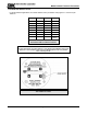
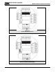
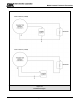
Transmitter External Interfaces (See Figure 3-2)
1. Establish the module address according to section 3.5.
NOTES
The starting delay period normally takes approximately 3 minutes but it depends on the sensor
connected.