
Specifications

- 9 -
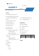
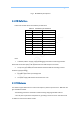
Fig 1 ML3369T-P pin sequence
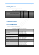
4.2. PIN Definitions
Please refer to Table 16 for the hardware pin definitions.
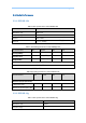
Table 16 ML3369T-P pin definitions
Pin
Function 1
Function 2
1
VDD
2
GND
3
GPIO8
PWM0
4
GPIO13
PWM1
5
GPIO0
PWM2
6
GPIO25
PWM3
7
GPIO3
PWT
8
GPIO6
ADC
9
UART_TX
GPIO27
10
UART_RX
GPIO26
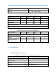
Note:
1. In default, UART is used for output of debugging information and burning firmware.
Please refer to the description in DC Characteristics for UART output current level.
2. The pins for reset button and LED indication should be defined according to actual
firmware and circuit design.
3. The ADC is 10-bit with input voltage 0-2V
4. The power supply VDD should not be lower than 3.3V.
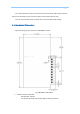
4.3. PCB Antenna
The module support PCB antenna in 2.4G~2.5G frequency with S11 port less than -10dB and max
gain of 0.6dB at 2.45GHz.
The following precautions should be considered during designing with PCB antenna:
1. Do not place any electrical components or grounding in antenna area on main board and
it’s better to leave this area blank on PCB.