RF-BM-BG22B1 EFR32BG22 Bluetooth 5.2 Low Energy Module Version 1.0 Shenzhen RF-star Technology Co., Ltd.
RF-BM-BG22B1 www.szrfstar.com 1 Device Overview 1.1 Module Series There are three modules of RF-BM-BG22Bx series. All of them are based on Silicon Labs EFR32BG22 series. Because the EFR32BG22 chips are compatible in package, pins and peripherals, those three modules are pin-to-pin compatible with each other as well. Table 1. Module Specification of RF-BM-BG22Bx Max. CPU TX Speed Power EFR32BG22C112F352GM32-C 38.4 MHz EFR32BG22C222F352GM32-C 76.
RF-BM-BG22B1 www.szrfstar.
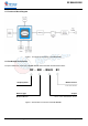
RF-BM-BG22B1 www.szrfstar.com 1.5 Functional Block Diagram Figure 1. Functional Block Diagram of RF-BM-BG22B1 1.6 Part Number Conventions The part numbers are of the form of RF-BM-BG22B1 where the fields are defined as follows: RF - BM - BG22 B1 Company Name Module Version RF-star The first version Wireless Type Bluetooth Module Chipset Silicon Labs EFR32BG22 Series Figure 2. Part Number Conventions of RF-BM-BG22B1 Shenzhen RF-star Technology Co., Ltd.
RF-BM-BG22B1 www.szrfstar.com Table of Contents 1 Device Overview ............................................................................................................................................................. 1 1.1 Module Series ..................................................................................................................................................... 1 1.2 Description....................................................................................................
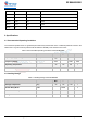
RF-BM-BG22B1 www.szrfstar.com 2 Module Configuration and Functions 2.1 Module Parameters Table 2. Parameters of RF-BM-BG22B1 Chipset EFR32BG22C112F352GM32-C Supply Power Voltage 2.2 V ~ 3.8 V, recommended to 3.3 V Frequency 2402 MHz ~ 2480 MHz Transmit Power -28.0 dBm ~ 0 dBm (typical: 0 dBm) Receiving Sensitivity Power Consumption -98.9 dBm sensitivity @ 1 Mbit/s GFSK -96.2 dBm sensitivity @ 2 Mbit/s GFSK 3.6 mA RX current (1 Mbps GFSK) 4.
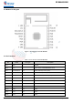
RF-BM-BG22B1 www.szrfstar.com 2.2 Module Pin Diagram Figure 3. Pin Diagram of RF-BM-BG22B1 2.3 Pin Functions Table 3. Pin Functions of RF-BM-BG22B1 Pin Name Pin Type Description Pin1 GND - Ground Pin2 VCC - 2.2 V ~ 3.8 V, recommended to 3.3 V Pin3 PA01/SWCLK I/O GPIO/SWCLK(connect jlink) Pin4 PA02/SWDIO I/O GPIO/SWDIO(connect jlink) Pin5 RESET I Reset, active low, internal pull-up.
RF-BM-BG22B1 www.szrfstar.com Pin13 PC05 I/O GPIO Pin14 PA05 I/O GPIO Pin15 PA06 I/O GPIO Pin16 PC00 I/O GPIO Pin17 PC01 I/O GPIO Pin18 NC - - 3 Specifications 3.1 Recommended Operating Conditions The functional operation does not guarantee performance beyond the limits of the conditional parameter values in the table below. Long-term work beyond this limit will affect the reliability of the module more or less. Table 4.
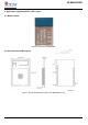
RF-BM-BG22B1 www.szrfstar.com 4 Application, Implementation, and Layout 4.1 Module Photos Figure 4. Photos of RF-BM-BG22B1 4.2 Recommended PCB Footprint Figure 5. Recommended PCB Footprint of RF-BM-BG22B1 (mm) Shenzhen RF-star Technology Co., Ltd.
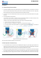
RF-BM-BG22B1 www.szrfstar.com 4.3 Antenna 4.3.1 Antenna Design Recommendation 1. The antenna installation structure has a great influence on the module performance. It is necessary to ensure the antenna is exposed and preferably vertically upward. When the module is installed inside of the case, a high-quality antenna extension wire can be used to extend the antenna to the outside of the case. 2.
RF-BM-BG22B1 www.szrfstar.com which is beneficial to the long-term stable operation of the whole machine. The module should be far away from the power electromagnetic, transformer, high-frequency wiring, and other parts with large electromagnetic interference. 4. The bottom of the module should avoid high-frequency digital routing, high-frequency analog routing, and power routing.
RF-BM-BG22B1 www.szrfstar.com 4.5.2 Vulnerable Module 1. Please ensure the supply voltage is between the recommended values. The module will be permanently damaged if the voltage exceeds the maximum value. Please ensure a stable power supply and no frequently fluctuated voltage. 2. Please ensure the anti-static installation and the electrostatic sensitivity of high-frequency devices. 3. Due to some humidity-sensitive components, please ensure suitable humidity during installation and application.
RF-BM-BG22B1 www.szrfstar.com Liquid Temperature (TL) 183 ℃ 217 ℃ Time above Liquidus (tL) 60 s ~ 90 s 30 s ~ 90 s 220 ℃ ~ 235 ℃ 230 ℃ ~ 250 ℃ Max. 6 ℃/s Max. 6 ℃/s Max. 6 minutes Max. 8 minutes 20±10 s 20±10 s Peak Temperature (Tp) Average Descend Rate (Tp to Tmax) Time from 25 ℃ to Peak Temperature (t2) Time of Soldering Zone (tP) Figure 7. Recommended Reflow for Lead-Free Solder Shenzhen RF-star Technology Co., Ltd.
RF-BM-BG22B1 www.szrfstar.com 4.8 Optional Packaging Figure 8. Optional Packaging Mode Note: Default tray packaging. 5 FCC Warning This device complies with Part 15 of the FCC Rules. Operation is subject to the following two conditions: (1) This device may not cause harmful interference. (2) This device must accept any interference received, including interference that may cause undesiredoperation. Shenzhen RF-star Technology Co., Ltd.
RF-BM-BG22B1 www.szrfstar.com 6 Revision History Date Version No. 2022.06.10 V1.0 Description The initial version is released. Note: 1. The document will be optimized and updated from time to time. Before using this document, please make sure it is the latest version. 2. To obtain the latest document, please download it from the official website: www.szrfstar.com. Shenzhen RF-star Technology Co., Ltd.
RF-BM-BG22B1 www.szrfstar.com 7 Contact Us SHENZHEN RF-STAR TECHNOLOGY CO., LTD. Shenzhen HQ: Add.: C601, Skyworth Building, High-tech Park, Nanshan District, Shenzhen, Guangdong, China, 518057 Tel.: 86-755-3695 3756 Chengdu Branch: Add.: N2-1604, Global Center, North No. 1700, Tianfu Avenue, Hi-Tech District, Chengdu, Sichuan, China, 610095 Tel.: 86-28-6577 5970 Email: sunny@szrfstar.com, sales@szrfstar.com Web.: www.szrfstar.com Shenzhen RF-star Technology Co., Ltd.
FCC Statement FCC standards: FCC CFR Title 47 Part 15 Subpart C Section 15.247 PCB antenna , Antenna gain 0dBi This device complies with part 15 of the FCC Rules. Operation is subject to the following two conditions: (1) This device may not cause harmful interference, and (2) this device must accept any interference received, including interference that may cause undesired operation.
—Increase the separation between the equipment and receiver. —Connect the equipment into an outlet on a circuit different from that to which the receiver is connected. —Consult the dealer or an experienced radio/TV technician for help. 2. Changes or modifications not expressly approved by the party responsible for compliance could void the user's authority to operate the equipment.