
Users Manual


RAK
4630
7
SWD Interface
Pin Name
Pin No.
Type
Description
Comment
SWDIO
19
Debug
SWD I/O for debug and
programming
SWCLK
18
Debug
SWD clock input for debug
and programming
RESET
Pin Name
Pin No.
Type
Description
Comment
RESET
17
DI
Reset the module
NFC Interface
Pin Name
Pin No.
Type
Description
Comment
NFC1
13
DI
NFC input 1
P0.09
NFC2
12
DI
NFC input 2
P0.10
Antenna Interface
Pin Name
Pin No.
Type
Description
Comment
RF_BT
15
IO
Bluetooth antenna
interface
50Ω Impedance
If unused, keep this pin open
GPIO Interface
Pin Name
Pin No.
Type
Description
Comment
GPIO P1.01
25
IO
General-purpose
input/output
GPIO P1.02
26
IO
General-purpose
input/output
GPIO P1.03
27
IO
General-purpose
input/output
GPIO P1.04
28
IO
General-purpose
input/output
ADC Interface
Pin Name
Pin No.
Type
Description
Comment
GPIO P0.31 / AIN7
39
IO / AI
General-purpose IO /
General purpose ADC
interface
GPIO P0.05 / AIN3
40
IO / AI
General-purpose IO /
General purpose ADC
interface
GPIO P0.04 / AIN7
41
IO / AI
General-purpose IO /
General purpose ADC
interface
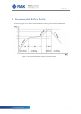
2.6
Power Consumption
The following table show the power consumption.
Table 4: Power Consumption
Item
P
owe
r
C
o
n
s
u
m
p
t
io
n
C
o
nd
i
t
io
n
Tx mode BT@4dBm
9mA
BT Tx mode
Rx
mode
BT@2Mbps
11.5mA
BT
Rx
mode
Sleep
mode
2.0uA
BT
sleep
2.7
Absolute Maximum Ratings
R
AK2011
R
AK2011