
User's Manual


Information in this document is subject to change without prior notice. Page 9 of 11
7.1. Power supply:
1) The input power can be 5.0VDC or 3.3VDC, please mentioned it when place an order.
2) The operation current of 5.0VDC power input will be different with that of 3.3V power
input. The external power shall be well designed with enough capacity.
3) Should 3.3VDC power be selected, please be sure it’s clean with low ripple; otherwise,
the EMI or RF performance might be deteriorated.
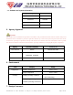
7.2. Using pin headers:
1) The pins can be less than 7 pins, but the VCC, UD-, UD+, GND must be applied for
USB interface communication.
2) Should the pin header connection be applied, please still keep enough metallic clear
space around the antenna end of the module, this gives better antenna performance
7.3. Using semi-holes:
1) When the module is designed to be soldered on a main PCB board directly, the area
under the antenna end of the module should be keep clear of metallic components,
connectors, vias, traces and other materials that can interfere with the radio signal.
2) The module is not recommended using reflow oven process, hand soldering is
suggested.
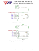
7.4. Footprint design reference:
The following drawing shows a recommended footprint which can be a reference design for a main
PCB layout.