M590 GPRS Module Hardware User Guide Version 1.
M590 GPRS Module Hardware User Guide Copyright © Neoway Technology Co., Ltd 2014. All rights reserved. No part of this document may be reproduced or transmitted in any form or by any means without prior written consent of Shenzhen Neoway Technology Co., Ltd. is the trademark of Neoway Technology Co., Ltd. All other trademarks and trade names mentioned in this document are the property of their respective holders.
M590 GPRS Module Hardware User Guide Revision Record Issue Changes Revised By Date V1.0 Initial draft Qiao Naiwei 2013-10 V1.1 Modified the description of VCCIO Qiao Naiwei 2014-04 V1.2 Added chapter 4. Weng Peibin 2014-05 Copyright © Neoway Technology Co.
M590 GPRS Module Hardware User Guide Contents About This Document ......................................................................................................... 1 1 Introduction to M590 ........................................................................................................ 1 1.1 Overview ..................................................................................................................................... 1 1.2 Block Diagram ........................................
M590 GPRS Module Hardware User Guide Table of Figures Figure 2-1 Top view of the M590 module ............................................................................................... 3 Figure 2-2 PCB foot print recommended for M590 (unit: mm) .............................................................. 6 Figure 3-1 Current peaks and voltage drops ............................................................................................ 7 Figure 3-2 Capacitors used for the power supply ...........
M590 GPRS Module Hardware User Guide Table of Tables Table 1-1 M590 specifications ................................................................................................................. 2 Table 2-1 M590 pin definition ................................................................................................................. 4 Table 3-1 Power supply and switch interface .......................................................................................... 7 Table 3-2 UART ..............
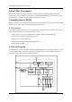
M590 GPRS Module Hardware User Guide About This Document This document defines the features, indicators, and test standards of the M590 module and provides reference for the hardware design of each interface. With M590 GPRS Module AT Command Set, this user guide can help you complete wireless communication application easily. 1 Introduction to M590 M590 is a compact wireless GPRS module that supports downlink EDGE.
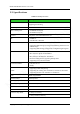
M590 GPRS Module Hardware User Guide 1.3 Specifications Table 1-1 M590specifications Specifications Description Band EGSM900/DCS1800 MHz dual-band Supporting band locking Sensitivity < -107 dBm Max. transmit power l EGSM900 Class4(2W) l DCS1800 Class1(1W) Protocol Compatible with GSM/GPRS Phase 2/2+ AT l GSM07.
M590 GPRS Module Hardware User Guide 2 Pin Description and PCB Foot Print 2.1 Specifications and Encapsulation Specifications M590 Dimensions 27.6 mm x 21.6 mm x 2.6 mm (H x W x D) Weight 2.
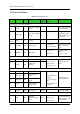
M590 GPRS Module Hardware User Guide 2.2 Pin Definition Table 2-1 M590 pin definition Pin Name I/O Function Reset Status Level (V) Feature Remarks Power Supply and Switch Interfaces 2, 3 VBAT P Main power supply input 3.5 V to 4.3 V (3.9 V is recommended) Supply power for IO level shifting circuit. Load capability: less than 50 mA 6 VDD_EXT P 2.8 V power supply output 1, 4, 15, 20 GND P Ground 19 ON/OFF DI On/Off input 18 RESET DI Reset input 0
M590 GPRS Module Hardware User Guide 2.38
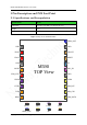
M590 GPRS Module Hardware User Guide 2.3 PCB Foot Print LCC packaging is adopted to package the pins of the M590 module. Figure 2-2 shows the recommended PCB foot print. Figure 2-2 PCBfoot print recommended for M590 (unit: mm) 21.6 4.0 2.35 3.4 2.54 Copper Cut D=2.0 Pads 1~20 : 1.8*2.4 Pad 21 : 1.2*1.6 27.6 M590 Pitch: X=21.2;Y=2.54 Unit:mm 21.2 Copyright © Neoway Technology Co.
M590 GPRS Module Hardware User Guide 3 Interface Design 3.1 Power Supply and Switch Interfaces Table 3-1 Power supply and switch interface Signal I/O Function Remarks VBAT P Main power supply input 3.5 V to 4.3 V (3.9 V is recommended) VDD_EXT P 2.8 V power supply output Loading capability < 50 mA RESET DI Module reset input Reset at low level Min. 50 ms 100 ms is recommended ON/OFF DI On/Off input Low level pulse can change the On/Off state. 3.1.
M590 GPRS Module Hardware User Guide Figure 3-2shows a recommended power supply design for the module. Figure 3-2 Capacitors used for the power supply In the circuit, you can use TVS at D1 to enhance the performance of the module during a burst. SMF5.0AG (Vrwm=5V&Pppm=200W) is recommended.A large bypass tantalum capacitor (220 μF or 100μF) or aluminum capacitor (470 μF or 1000 μF) is expected at C1 to reduce voltage drops during bursts together with C2 (10μF capacitor). In addition, you need to add 0.
M590 GPRS Module Hardware User Guide Figure 3-4 Reference design of power supply controlled by p-MOSFET Q1 VCC_IN_3.9V S VBAT D C3 C1 C2 10 uF 0.1 uF R4 G R3 GPRS_EN TVS 5V 100K C4 C5 C6 470 uF 10 uF 0.1 uF 100pF C7 33 pF 10K R1 Q2 2K R2 10K Q2 is added to eliminate the need for a high enough voltage level of the host GPIO.In case that the GPIO can output a high voltage greater than VCC_IN_3.9V - |VGS(th)|, where VGS(th) is the Gate Threshold Voltage, Q2 is not needed.
M590 GPRS Module Hardware User Guide separated power supplies.The module shall be supplied by an independent power, like a DC/DC or LDO. See Figure 3-5. DC/DC or LDO should output rated peak current larger than 2 A. The inductor used in Reference Design (b), should be a power inductor and have a very low resistance. 10 uH with average current ability greater than 1.2A and low DC resistance is recommended.
M590 GPRS Module Hardware User Guide Figure 3-6 Power-on procedure VBAT 3s 1.2s ON/OFF 300 ms VDD_EXT UART Power-Off Procedure While the module is on, drive the ON/OFF pin to ground for at least 500 ms and then release, the module will try to detach to network and normally 2 seconds later it will shut down. Another approach to turn off the module is using AT commands. For details, see M590 GPRS Module AT Commands. Figure 3-7 shows the power-off procedure of the module.
M590 GPRS Module Hardware User Guide Figure 3-8 Reference circuit for power-on/off control ON/OFF S1 GPRS Module TVS Figure 3-9 Reference circuit for power-on/off controlled by high level ON/OFF 4.7K R1 GPRS Module USER_ON R2 47K In Figure 3-9, high level takes effect for ON/OFF on the user side (USER_ON) after level shifting. R1 and R2 can be adjusted according to the driving capability of the USER_ON pin. Use a common NPN transistor, e.g. MMBT3904; or a digital NPN transistor, e.g. DTC123.
M590 GPRS Module Hardware User Guide 3.1.4 RESET You can reset the module by keeping the RESET pin low level for more than 100 ms.The pin is pulled up by an internal resistor and the typical high level is 2.8 V. The RESET pin can be left disconnected if not used. If you use 3.3 V IO system, you are advised to separate it by using triode. Please refer to Figure 3-10. Figure 3-10 Reset circuitwith triode separating VDD_EXT 4.7K 47K GPRS Module RESET 3.
M590 GPRS Module Hardware User Guide If the UART is interfacing with a MCU that has 3.3V logic levels, it is recommended that you add a level shifting circuit outside of the module. Figure 3-12 Recommended circuit for the communication between 3.3V MCU and UART VDD_EXT 0.1 uF 47K MCU_UTXD Module_URXD RB521S 33 pF 200 MCU_URXD Module_UTXD 33 pF In Figure 3-12, 100 pF filter capacitor should be placed near the receive pin of the module.
M590 GPRS Module Hardware User Guide In Figure 3-13, INPUT is connected to UTXD of the MCU and VCC_IN is connected to the 5 V power supply of the MCU. OUTPUT is connected to URXD of the module and VCC_OUT is connected to VDD_EXT(2.8V) of the module.If the circuit is far away from the VDD_EXTpin, add a 0.1 μF decoupling capacitor to VCC_OUT. Level shifting between URXD of the MCU and UTXD of the module can be implemented in the same way. The pull-up resistor R3 ranges from 4.
M590 GPRS Module Hardware User Guide 4. Pull DTR high, the module will exit from sleep mode actively, and furthermore enable the UART. Thus the voice call, received data, or SMS can be processed through UART.After processing finished pull it low again, to take the module back to sleep mode. 3.3.2 RING Signal Indicator l Calling: Once a voice call is coming, UART output "RING" character strings and meanwhile the RING pin outputs 30 ms low pulses at 5s period.
M590 GPRS Module Hardware User Guide Figure 3-16 Reference design of SIM card interface 20 SIM_DATA 20 SIM_CLK 20 SIM_RST VSIM GPRS Module CLK DATA RST VPP VCC GND 1 uF SIM卡 ESD protectors, such as ESD diodes (lower than 33 pF) or ESD varistors, are recommended on the SIM signals, especially in automotive electronics or other applications with badly ESD. ESD.In In other applications, replace ESD diodes with 27 pF to 33 pF grounding capacitors.
M590 GPRS Module Hardware User Guide SIM card is sensitive to GSM TDD noise and RF interference. So, the PCB design should meet the following requirements: l The antenna should be installed far away from the SIM card and SIM card traces, especially to the build-in antenna. l The SIM traces on the PCB should be as short as possible and shielded with GND copper. l The ESD diodes or small capacitors should be closed to SIM card on the PCB. 3.
M590 GPRS Module Hardware User Guide 3.6 RF Interface 3.6.1 RF Design and PCB Layout A 50 Ω antenna is required. VSWR ranges from 1.1 to 1.5. The antenna should be well matched to achieve best performance. It should be installed far away from high speed logic circuits, DC/DC power, or any other strong disturbing sources. For multiple-layer PCB, the trace between the antenna pad of module and the antenna connector, should have a 50 Ω characteristic impedance, and be as short as possible.
M590 GPRS Module Hardware User Guide Figure 3-20 RF layout reference Ensure complete ground at both sides of the 20th pin. Avoid ground at only one side. The RF route should be as short and smooth as possible and at a width of 1 mm; the RF is 1 mm away from the ground. Separate the copper-removing area from the RF route by ground. Remove the copper from the top layer of the RF testing point (2mm in diameter). Dig ground holes around this are.
M590 GPRS Module Hardware User Guide 3.6.2 Recommended RF Connection If you adopts RF cables for connections, the GSC RF connector MM9329-2700RA1 from Murata is recommended. Figure 3-22 shows the encapsulation specifications. Figure 3-22 Encapsulation specifications of Murata RF connector Copyright © Neoway Technology Co.
M590 GPRS Module Hardware User Guide 4 Electric Features and Reliability 4.1 Electric Feature Table 4-1 Electric feature of the module Parameter Minimum Value Typical Value Maximum Value Vin 3.5V 3.9V 4.3V Iin / / 2A Vout / 2.8V / Iout / / 50mA Vout 2.3V 2.8V 3.1V Iout / / 4mA Vin -0.3V 0V 0.6V Iin / / 22.5uA VBAT VDD_EXT DIO If the voltage is too low, the module might fail to start.
M590 GPRS Module Hardware User Guide 4.3 Current Table 4-3 Current feature Parameter Testing Conditions Testing Result (Average Current) Testing voltage 3.9 V Agilent power supply / Idle mode Set the instrument and power on the module. 18mA Off leakage current Power on the module or use AT command to shut the module down. 50uA Average network searching current Sleep mode Voice service Set the instrument. Start the module. Wait until the module registers the instrument.
M590 GPRS Module Hardware User Guide ANT ±8KV ±15KV Cover ±8KV ±15KV URXD/UTXD ±4KV ±8KV Others ±4KV ±8KV Copyright © Neoway Technology Co.
M590 GPRS Module Hardware User Guide 5 RF Features 5.1 Work Band Table 5-1 Work band Work Band Uplink Downlink EGSM900 880~915MHz 925~960MHz DCS1800 1710~1785MHz 1805~1880MHz 5.2 Transmitting Power and Receiving Sensitivity 5.2.
M590 GPRS Module Hardware User Guide 2 26 dBm ±3dBm 3 24 dBm ±3dBm 4 22 dBm ±3dBm 5 20 dBm ±3dBm 6 18 dBm ±3dBm 7 16 dBm ±3dBm 8 14 dBm ±3dBm 9 12 dBm ±3dBm 10 10 dBm ±4Bm 11 8 dBm ±4Bm 12 6 dBm ±4Bm 13 4 dBm ±4dBm 14 2 dBm ±5dBm 15 0 dBm ±5 dBm 5.2.2 Receiving Sensitivity Band Typical GSM800&EGSM900 <-107 dBm DCS1800&PCS1900 <-107 dBm The data in the above tables is obtained by connecting the module to RF test instrument (e.g.
M590 GPRS Module Hardware User Guide 6 Mounting the Module onto the Application Board M590 is compatible with industrial standard reflow profile for lead-free SMT process. The reflow profile is process dependent, so the following recommendation is just a start point guideline: l Only one flow is supported. l Quality of the solder joint depends on the solder volume. Minimum of 0.15mm stencil thickness is recommended. l Use bigger aperture size of the stencil than actual pad size.
M590 GPRS Module Hardware User Guide 8 Abbreviations ADC Analog-Digital Converter AFC Automatic Frequency Control AGC Automatic Gain Control AMR Acknowledged multirate (speech coder) CSD Circuit Switched Data CPU Central Processing Unit DAI Digital Audio interface DAC Digital-to-Analog Converter DCE Data Communication Equipment DSP Digital Signal Processor DTE Data Terminal Equipment DTMF Dual Tone Multi-Frequency DTR Data Terminal Ready EFR Enhanced Full Rate EGSM Enhanced GSM
M590 GPRS Module Hardware User Guide RAM Random Access Memory RF Radio Frequency ROM Read-only Memory RMS Root Mean Square RTC Real Time Clock SIM Subscriber Identification Module SMS Short Message Service SRAM Static Random Access Memory TA Terminal adapter TDMA Time Division Multiple Access UART Universal asynchronous receiver-transmitter VSWR Voltage Standing Wave Ratio Modular Approal: The M590 module is designed to comply with the FCC statement. FCC ID is PJ7-125X.
M590 GPRS Module Hardware User Guide terference to radio communications. However, there is no guarantee that interference will not occur in a particular installation. If this equipment does cause harmful interference to radio or television reception, which can be determined by turning the equipment off and on, the user is encouraged to try to correct t he interference by one or more of the following measures: -Reorient or relocate the receiving antenna.