
User's Manual


Shenzhen Neoway Technology Co., Ltd. Page 9 of 32
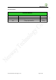
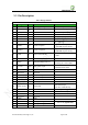
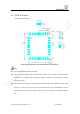
5.3 Pin Description
Table2 M660 pin definition
M660
Pin
Signal
I/O
Function
Note
1
VSIM
PWR
SIM supply voltage
1.8/3.0V compatible.
2
SIM_CLK
DO
SIM clock
3
SIM_DATA
DIO
SIM data
5KΩ internal pull-up
4
GND
PWR
GND
5
SIM_RST
DO
SIM reset
Prompted by module
6
MICP
AI
MIC+
Vi ≤ 200mVpp
7
MICN
AI
MIC-
Vi ≤ 200mVpp
8
EAR-L
AO
Earpiece output L
Signal Ended Output. Can drive
a 16Ω/32Ω earpiece directly.
9
EAR-R
AO
Earpiece output R
Signal Ended Output. Can drive
a 16Ω/32Ω earpiece directly.
10
DTR
DI
Data Terminal Ready
Can be used to control sleep
mode.
11
GND
PWR
GND
12
RING
DO
Output for RING indicator
Can be used to indicate an
incoming voice call or SMS.
13
VCCIO
PWR
2.8V power output
Can be used to power the level
translators. Imax=5mA
14
Reserved
Reserved
15
Reserved
Reserved
16
URXD1
DI
Serial data input of module
V.24: TXD
17
UTXD1
DO
Serial data output of module
V.24: RXD
18
GND
PWR
GND
19
RESET
DI
Reset input
Active low > 60mS
20
BACK_LIGHT
DO
Status LED
2.8V/4mA output
Can drive a LED directly
21
ON/OFF
DI
Switch the module on/off
Low level pulse triggered
22
ANT
I/O
Antenna interface
A 50ohm antenna expected
23
GND
PWR
GND
24
Reserved
Reserved
25
GND
PWR
GND
26
VBAT
PWR
Main power supply
3.5V~4.3V (typical 3.9V)
27
VBAT
PWR
Main power supply
28
GND
PWR
GND