
User's Manual

Shenzhen Neoway Technology Co., Ltd. Page 28 of 32
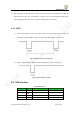
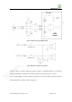
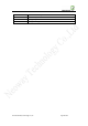
Figure 24 Reference layout for antenna interface
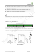
7. Mounting the Module onto the Application Board
M660 is compatible with industrial standard reflow profile for lead-free SMT process.
The reflow profile is process dependent, so the following recommendation is just a start point
guideline:
Only one flow is supported.
Quality of the solder joint depends on the solder volume. Minimum of 0.15mm stencil thickness
is recommended.
Use bigger aperture size of the stencil than actual pad size.
Use a low-residue, no-clean type solder paste.
This GND Pad
should be well
routed to ground
Antenna pad
should be
surrounded by
ground
Antenna trace should be surrounded by
ground which is connected to main
ground plane with plenty of via holes.
The trace width and the space to ground
should be decided by calculating of 50Ω
impedance match.