
User's Manual

Shenzhen Neoway Technology Co., Ltd. Page 10 of 32
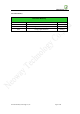
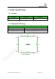
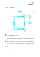
5.4 PCB foot print
Recommended foot print:
Figure 3 Recommended foot print of M660 (all dimensions in millimeters)
Note:
Every other pitch not specified is 2.0mm.
The circle on the top-right with a 1.3mm radius, defines a keep-out region, under which any
copper or wire is inhibited, due to the RF test point here needs to be surrounded by restricted
area filled with air.
There may be some masks on the bottom of the module PCB, created by hollowing the solder
resist layer, causing reveal of copper. To avoid short circuits, it is recommended to cover the
application PCB with a silkscreen block at the area under the module, but excluding soldering
area.