
User's Manual
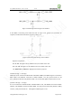
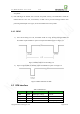
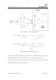
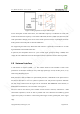
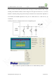
Table Of Contents
- 1. Introduction
- 2. General Description
- 3. Simplified Block Diagram
- 4. Key Features
- 5. Product Specifications
- 6. Application Interface
- 7. Mounting the Module onto the Application Board
- 8. Package
- 9. Terms and Abbreviations

Neo_M680 Hardware User Guide V1.0
Copyright Neoway Techlology Co., Ltd. Page 30 of 31
Figure 24 Reference layout for antenna interface
7. Mounting the Module onto the Application Board
M680 is compatible with industrial standard reflow profile for lead-free SMT process.
The reflow profile is process dependent, so the following recommendation is just a start point
guideline:
Only one flow is supported.
Quality of the solder joint depends on the solder volume. Minimum of 0.15mm stencil thickness
is recommended.
Use bigger aperture size of the stencil than actual pad size.
Use a low-residue, no-clean type solder paste.
8. Package
M680 modules are packaged in sealed bags on delivery to guarantee a long shelf life. Package the
modules again in case of opening for any reasons.
If exposed in air for more than 48 hours at conditions not worse than 30°C/60% RH, a baking
procedure should be done before SMT. Or, if the indication card shows humidity greater than 20%,
This GND Pad
should be well
routed to ground
Antenn
a trace should be surrounded by
ground which is
connected to main
ground plane with plenty of via holes.
The trace width and the space to ground
should be decided by calculating of 50Ω
impedance match.