
User's Manual
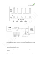
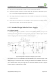
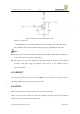
Table Of Contents
- 1. Introduction
- 2. General Description
- 3. Simplified Block Diagram
- 4. Key Features
- 5. Product Specifications
- 6. Application Interface
- 7. Mounting the Module onto the Application Board
- 8. Package
- 9. Terms and Abbreviations

Neo_M680 Hardware User Guide V1.0
Copyright Neoway Techlology Co., Ltd. Page 16 of 31
Figure 7 Using PMOS for power control
Q2 is for eliminating the need for a high enough voltage level of the host GPIO. In case that the
GPIO can output a high voltage greater than VDD3V9 - |V
GS(th)
|, where V
GS(th)
is the Gate Threshold
Voltage, Q2 is not needed.
Reference components:
Q1: IRML6401
Q2: MMBT3904
C4: 470uF tantalum capacitor rated at 6.3V; or 1000uF aluminum capacitor.
It’s strongly recommended to place a TVS diode on VBAT to ground, in order to absorb the power
surges subjected. The SMAJ5.0A from Vishay can be as a choice.
6.1.2.2 Power Separating
As described in section 6.1.1, the GSM device works in burst mode generating voltage drops on
power supply. And furthermore this results in a 217Hz TDD noise through power (One of the way
generating noise. Another way is through RF radiation). Analog parts, especially the audio circuits,
are subjected to this noise, known as a “buzz noise” in GSM systems. To prevent other parts from
being affected, it’s better to use separated power supplies. The module shall be supplied by an