
User's Manual
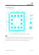
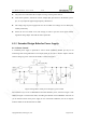
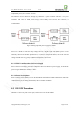
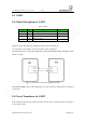
Table Of Contents
- 1. Introduction
- 2. General Description
- 3. Simplified Block Diagram
- 4. Key Features
- 5. Product Specifications
- 6. Application Interface
- 7. Mounting the Module onto the Application Board
- 8. Package
- 9. Terms and Abbreviations

Neo_M680 Hardware User Guide V1.0
Copyright Neoway Techlology Co., Ltd. Page 12 of 31
5.4 PCB foot print
Recommended foot print:
Figure 3 Recommended foot print of M680 (all dimensions in millimeters)
Note:
There may be some masks on the bottom of the module PCB, created by hollowing the solder resist
layer, causing reveal of copper. To avoid short circuits, it is recommended to cover the application
PCB with a silkscreen block at the area under the module, but excluding soldering area.