
User's Manual
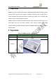

Neo_GM650 User Manual V1.0
All rights reserved by Shenzhen Neoway Technology Co., Ltd Page 9 Total 14
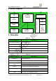
5 Pin Definition & Encapsulation
5.1 Pin Definition
The signal connection uses 74pin SMD pad of stamp hole(half hole).
Note: GM650 module IO interface level is 2.8V.
Because the module IO uses 2.8V power supply system, the maximum input voltage of all
the IO interface can not exceed the maximum 3.3V, otherwise it may damage the module
IO. Considering the signal integrality designing reasons,while the external circuit use 3.3V
power system the IO interface output voltage will exceed 3.3V because of overshoot
phenomenon, sometimes can even reach 3.5V.Therefore,the IO pin of the module will be
damaged if 3.3V IO signal is connected to 2.8V IO of the module directly.So it is needed to
adopt level matching measures.Please refer to chapter 6.2.
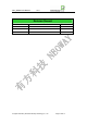
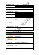
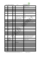
Table 5-1 GM650
Pin Definition
Pin
Signal Name
I/O Function Description
Remark
1 GND
PWR
Ground
2 Reserved
Reserved
3 Reserved Reserved
4 URXD1 DI UART1 data receiving
5
UTXD1
DO
UART1 data transmitting
Used to GPRS communications
and AT commands
6 NC
Reserved
suspend, without any signal input.
7 UTXD2
DO
UART2 data
transmitting, baud rate
= 9600
Dual-port mode, used to receive
GPS data;
Single-port mode, suspend.