
Specifications
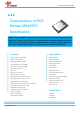
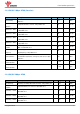
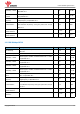
Table Of Contents

Copyright © Minew
8
m1805 Module Specification
3.2 Recommended operating conditions
Symbol
Parameter
Min.
Nom.
Max.
Units
VDD3
supply voltage,normal mode
1.8
3.0
3.6
V
tr_VDD
Supply rise time (0 V to 1.8 V)
100
ms
TA
Operating temperature
-40
27
125
°C
Important : The On-chip power-on reset circuitry may not function properly for rise times longer
than the specified maximum.
3.3 Electronic characteristic
3.3.1 General radio characteristics
Parameter
Description
Min.
TYP
Max.
Units
Tx only at 0dBm
With internal DC-DC @ 3V
8
mA
Rx only
With internal DC-DC @ 3V
8
mA
3.3.2 Radio current consumption (Transmitter)
Parameter
Description
Min.
Typ.
Max.
Units
RF Max output Power
10
dBm
RF Min Output Power
-20
dBm
OBW for BLE 1Mbps
20dB occupy-bandwidth for BLE modulation 1Mbps
1100
kHz
OBW for BLE 2Mbps
20dB occupy-bandwidth for BLE modulation 2Mbps
2300
kHz
OBW for GFSK 500 kbps
20dB occupy-bandwidth for GFSK modulation 2Mbps
1100
kHz
OBW for GFSK 125 bps
20dB occupy-bandwidth for GFSK modulation 2Mbps
1100
kHz
Error Vector Measure
Offset EVM for OQPSK modulation
0.02
FDEV for BLE 1Mbps
Frequency deviation for GFSK modulation 1Mbps
160
250
kHz
FDEV for BLE 2Mbps
Frequency deviation for GFSK modulation 2Mbps
320
500
kHz