
Specifications
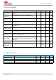
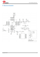
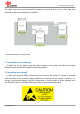
Table Of Contents

Copyright © Minew
16
m1805 Module Specification
7. Notes & cautions
We cannot assure that the specification has no errors and omission even though this specification
is under collate and check strictly.
This specification is under the protection of laws and regulations of copyright, please do not copy
and duplicate at any form, or do not transmit part or full of this specification in any wire and wireless
network in any form, or do not edit or translate to any other format, word, code, etc.
7.1 Design notes
(1) It is critical to following the recommendations of this document to ensure the module meets
the specifications.
(2) The module should be placed at the edge of the circuit board as far as possible to keep away
from other circuits.
(3) Antenna should be kept away from other circuits. It can prevent low radiation efficiency and
the normal use of other circuits from being affected.
(4) The landing of components should be appropriate and that is better for reducing the parasitic
inductance.
(5) Please refuse to supply voltage that is not within the range of specification.
(6) Please make sure the module or its surface may not suffer from the physical shock or
extreme stress.
7.2 Layout notes
To make sure wireless performance is at its best condition, please layout the module on the carrier
board as below instructions and picture.
(1) Placement of the antenna
The antenna area of module shall lay clearance completely and should not be blocked by the metal.
Otherwise it will have effect on antenna performance (As the picture indicated below).
(2) Placement of top-layer
The placement of top-layer in carrier board shall be lay copper completely to reduce the signal line
in carrier board or other interference.
(3) Clearance