
User Manual
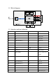
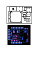
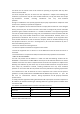

1.2 Block diag
r
am
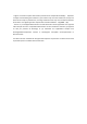
1.3 Interface and pin definition
No.
Pin name Type description
1 to 8
NC / No use
9
DC I Debug clock
10
DD O Debug data
11
SLEEP_OUT/P3_0 O Wakeup out
12
VDD Power Power in
13
GND Power ground
14
Reset RSTN Reset in
15
Wake/P0_3 I Wake up input
16
UART_RXD0 I Uart in, baud rate is
115200
17
UART_TXD0 O Uart out, baud rate is
115200
18
nCS1/CTSn1/P1_2 I/O Reserved
19
CLK1/RTSn1/P1_3 I/O Reserved
20
MOSI1/TXD1/P1_1 I/O Reserved
21
MISO1/RXD1/P1_0 I/O Reserved
22
CD O Module detect pin