
User's Manual

8
Circuit Description
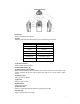
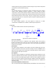
1. Power Supply
Power supply of the radio is derived from the battery, which supplies battery B+ after
passing through fuse 3A and then feeds through power switch. The power supplies
voltage for three AVRs. IC505 supplies 5V (5M) voltage for the control circuit. IC9
supplies 5V (5C) voltage for the shared circuit. And IC6 supplies voltage for the
transmit/receive circuit. In transmit mode, 5TC becomes low voltage and Q3 is turned
on to supply 5V(5T) voltage for the transmit circuit. In receive mode, 5RC becomes
low voltage and Q2 is turned on to supply 5V (5R) voltage for the receive circuit.
BATT FUSE
PROTECT
5C
5M
BUFF
1/2BIA
S
AVR
AVR
SW
5R
5T
AVR
SW
SW
SAVE
5RC
5TC
Fig. 1 Power Supply Block Diagram
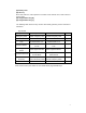
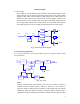
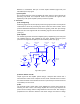
2. PLL Frequency Synthesizer
PLL circuit generates the first local oscillator signal for reception and RF signal
for transmission.
CPU
Q416
UL
X401
IC400
PLL
IC500
CV
CLK,DAT,EN
TCXO
VCO
BUFF SW
MB
D100
T/R
To Drive Amp
BUFF
D103
SW
To Mixer
Q310
Fig2. PLL circuit
1) PLL
IC400 is fractional divider. Step frequency of PLL circuit is 2.5KHz or 6.25KHz. A
16.8MHz reference oscillator signal is divided at IC400 by a fixed counter to
generate a 20KHz or 50KHz reference frequency. Output signal from VCO is buffer
amplified by Q416 and divided at IC400 by a frequency divider. Divided signal is
compared in the phase comparator with 20KHz or 50KHz reference signal of IC400.