
User's Manual

11
output from IC100 (1/2). The output voltage controls FET power amplifier and keeps
the transmitter output power constant. The output voltage can be varied by the
microprocessor, which hence controls the transmitter output power.
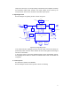
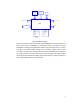
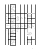
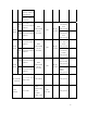
5. Signalling Section
The block diagram of signaling section is shown as figure 5.
D601
LIMITTER
X601
BASEBAND PROCESSOR
IC601
BBP_IRQN
BBP_RPL
SP
MIC
SW
Q700
AF PA
IC710
SW
Q710
MIC
AUDIO_EN
EXT_SPK+
EXT_MIC
BBP_CSN
BBP_CMD
BBP_CLK
Q701
SW
EXT_MIC_SEL
EXT_SP_SEL
IC605
BUFFER
Ver
Vbias
COMPANDER
IC603
SW
COM_SW EXP
EXP_SW
IC604
MOD
MB
COMPRESSOR EXPANDER
AF PA
MIC_FB
AUDIO
SW
COM
IC606
BUFF AMP
Vbias
IC611
FILTER
AF DET
Fig.5 AF and Signalling Circuit
In the transmit section, signallings (CTCSS, CDCSS, DTMF, 2-Tone and 5-Tone) are
produced by IC601 under the control of MCU and enter VCO together with AF signal
from MIC for modulation.
In the receive section, after buffer amplified together with IF demodulation signals,
the signallings enter IC601 for decode. The decoded data is then sent to MCU for
recognition.
6. Control System
The IC500 CPU operates at 9.8304MHz.
The block diagram of MCU control system is shown as following: