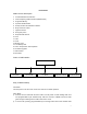
Content General Brief Introduction Radio Modes Circuit Description CPU Pins Adjustment Description TC3000-U Part List (Control Board) TC3000-U Part List (RF Board) TC3000-V Part List (Control Board) TC3000-V Part List (RF Board) Disassembly and Assembly for Repair Exploded View Part List 2 Packing TC3000-U PC Board View TC3000-V PC Board View TC3000 Block Diagram TC3000-U Schematic Diagram TC3000-V Schematic Diagram Specification 1
General Manual Scope This manual is intended for use by experienced technicians familiar with similar types of communication equipment. It contains all service information required for the equipment and is current as of the publication date. User Safety Information The following precautions are recommended for personnel safety: DO NOT transmit until all RF connectors are verified secure and any open connectors are properly terminated.
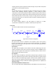
Brief Introduction (1) Antenna Used to transmit/receive signals. (2) LED Following table indicates LED indication and corresponding radio status. LED No display Status Standby Green Receive Red Transmit Flashing green Scan Flashing red Low battery voltage Flashing orange Call waiting (3) Channel Selector Used to select wanted channel.
(11) Battery Pack (12) PTT key Press and hold PTT, radio operates in transmit mode. Release PTT, radio returns to receive mode.
Radio Modes Radio Feature Description 1. 2. 3. 4. 5. 6. 7. 8. 9. 10. 11. 12. 13. 14. 15. 16. 17. 18. CTCSS/CDCSS/2-Tone/5-Tone Channel Spacing 25KHz/12.
directly through UART port. During cloning, LED of source radio flashes red and that of target radio flashes green. A BEEP sounds when cloning is complete. PC Mode 1) Connect the radio with a PC by programming cable. And then turn the power on. The radio enters PC mode after two seconds and LED glows orange. 2) Data can be transferred between MCU and PC via UART port. If data is transferred to the radio from PC, it can be programmed into the EEPROM by MCU and LED flashes red during data transfer.
CH5: Low power; CH6: CDCSS balance; CH7: Maximum frequency deviation; CH8: MIC sensitivity; CH9: CTCSS deviation; CH10: CDCSS deviation; CH11: FFSK deviation; CH12: TONE deviation; CH13: Receiving sensitivity; CH14: Squelch level; CH15: Low battery alert level; CH16: VOX sensitivity.
Circuit Description 1. Power Supply Power supply of the radio is derived from the battery, which supplies battery B+ after passing through fuse 3A and then feeds through power switch. The power supplies voltage for three AVRs. IC505 supplies 5V (5M) voltage for the control circuit. IC9 supplies 5V (5C) voltage for the shared circuit. And IC6 supplies voltage for the transmit/receive circuit. In transmit mode, 5TC becomes low voltage and Q3 is turned on to supply 5V(5T) voltage for the transmit circuit.
Output signal from phase comparator is filtered through a low pass filter and passed to the VCO to control oscillator frequency. 2) VCO The operating frequency is generated by Q352 in transmit mode and by Q350 in receive mode. Operating frequency generates a control voltage by phase comparator to control varactor diodes so that the oscillator frequency is the same as the MCU preset frequency (D350, D352, D354 and D355 in transmit mode and D351, D353, D356 and D357 in receive mode).
wideband or narrowband. W/N pin of IC500 outputs wideband (high level) and narrowband (low level) signal. 5) AF Amplifier The result AF signal from IC204 is amplified by IC606, and then passes through AF processing chip IC601 and compander IC603. The processed AF signal is then amplified by an AF power amplifier (IC720) to drive the speaker. 4. Transmitter 1) AF and Signaling Modulating signal from the microphone passes through Q700 switch and compander IC603 before it enters AF processing chip IC601.
output from IC100 (1/2). The output voltage controls FET power amplifier and keeps the transmitter output power constant. The output voltage can be varied by the microprocessor, which hence controls the transmitter output power. 5. Signalling Section The block diagram of signaling section is shown as figure 5.
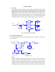
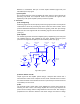
E2PROM RESET FLASH CTC/CDC Codec AF Processor MCU TXD/RXD PLL IC APC/TV SAVE BEEP LED AP SW MUTE 5TC 5RC W/N T/R I/E CH Encode VOL Level BATT Det KEY SW PTT RSSI Fig.6 MCU Block Diagram Circuit in this section is mainly comprised of MCU, EEPROM, FLASH and reset IC etc.
CPU Pins No.
40 P54 NULL NC 41 P53 NULL NC 42 P52 43 P51 44 P50 O WE 45 P47 I OPTION2 External accessory select 46 P46 I OPTION1 External accessory select O OE NULL Flash data output enable, active low NC Flash data input enable, active low Transmit/receive PLL select 47 P45 O T/R H: receive 48 P44 O CE Flash chip select, active low 49 P43 50 P42 O A18 Flash address 51 P41 O A17 Flash address 52 P40 O A16 Flash address 53 P37 O A15 Flash address 54 P36 O A1
79 P07 I/O D7 Flash data 80 P06 I/O D6 Flash data 81 P05 I/O D5 Flash data 82 P04 I/O D4 Flash data 83 P03 I/O D3 Flash data 84 P02 I/O D2 Flash data 85 P01 I/O D1 Flash data 86 P00 I/O D0 Flash data 87 P107 I EN3 Channel selector knob input 88 P106 I EN2 Channel selector knob input 89 P105 I EN1 Channel selector knob input 90 P104 I CTCSS_IN 91 P103 I BATTD 92 P102 I SQL Squelch level input (analogue) 93 P101 I RSSI RSSI detect pin (an
Adjustment Description Required Test Instrument Radio communication test set Scanner 3A/10V power supply Digital voltmeter 3A Ammeter 1 set 1 set 1 set 1 set 1 set Preparation Open the programming software in PC and operate as the following instructions. 1. Programme Download: Connect the radio with the computer via programming cable. And then turn the power on. LED glows red. Click “Programme” → “Download” on the interface to choose programme. Click “Open” to begin download and LED flashes red.
Transmitter Item Measurement Condition Test Instrument 1. Transmit Turn to CH3. frequency Press PTT. Terminal Radio Communication ANT Test Set Adjustment Part [B] (up) [C] (down) frequency. Press [A] to save. Press PTT. I≤1.6A. Center frequency Press [A] to save. Press PTT. high frequency. Adjust to 4.0 W, Radio Communication 1. Turn to CH5. Test Set Press PTT. Ammeter 4.0W±0.3W I≤1.6A. ANT [B] (up) Press [A] to save. [C] (down) Adjust to 1.0 W, I≤0.7A. Center frequency.
4. Press [A] for two seconds. LED flashes indicating radio that the operates with narrowband. Center frequency. Adjust narrowband following the above steps. 1. Turn to CH7. Wideband 4. Maximu- frequenc deviation The radio band Communication Test Set seconds. LED flashes LPF: 15KHz radio that operates to Press [A] to save. Radio 2. Press [A] for two Narrow- indicating it 4.0KHz±100Hz. operates with wideband. Center frequency. m -y Adjust Press PTT.
5. Press PTT. Frequency changes to center frequency. 6. Press PTT. Frequency changes to low frequency. Wideband 7. See CTCSS deviation adjustment. CDCSS deviation Adjust deviation Turn to CH10. to 0.70KHz± Radio Communication Test Set Narrowb See CTCSS deviation -and 50Hz. ANT [B] (up) Press [A] to save. [C] (down) Adjust deviation LPF: 3KHz to 0.35KHz± adjustment. 50Hz. Press [A] to save. Turn to CH11. Adjust deviation Wideba- See CTCSS deviation to 3KHz± nd adjustment. 8.
Receiver Item Measurement Condition Test Instrument 1. Turn to Adjustment Terminal Part ANT [B] (up) T1 [C] (down) Specification/ Remarks Method CH13. Press PTT. Center frequency. 2. Sensitivity Press PTT. Frequency changes to Scanner low frequency. 3. Press Adjust the waveform. Press [A] to save. PTT. Frequency changes to high frequency. 1. Turn to CH14. Press PTT. The Radio radio operates Communication with wideband. Wideband Test Set Center frequency. 2. Press PTT.
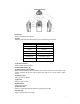
Disassembly and Assembly for Repair Disassemble the radio 1. Turn off the radio. 2. Remove the battery: a. Press the release at top of the battery downwards. b. Separate top of the battery from the radio. c. Lift the battery off. (See fig.1) 电池推钮 Battery Latch Fig. 1 3. Remove the antenna. 4. Remove the knob. (See fig.2) Fig. 2 5. Separate the chassis from PCB: a. Insert a screwdriver (Material No. 99050312) into the clearance between chassis and the case. b.
6. Remove the main PCB: a. Remove the two screw caps on top of the unit. b. Remove the five screws between PCB and the chassis. c. Loosen the weld between antenna pedestal and PCB using a soldering iron. d. Lift the PCB off. (See fig.4) Fig.4 7. Remove the small PCB: Loosen the screw to remove the small PCB. And then loosen the socket of flexible PCB. (See fig.5) Fig.5 8. Disassemble PTT key: Push the tab on PTT out of the hole on the case to disassemble PTT key. (See fig.6) Fig.6 Assemble the radio 1.
Fig.7 2. Assemble the small PCB: a. Insert the flexible PCB into the socket on the small PCB and lock it up. b. Insert the bottom of the small PCB into the underside of the two tabs under the case. c. Tighten the screws. (See fig.8) Fig.8 3. Assemble the chassis and PCB a. Insert the switch shaft in front of the PCB into the corresponding holes on the case. b. Press the bottom of the chassis downwards until a click is heard. (See fig.9) Fig.9 4. Attach the battery: a.
Exploded View 24
Packing Owner ' s Manual Power Suppl y Cor d Bel t Cl i p Bat t er y Adapt er St r ap Char ger Ant enna Mai n Uni t Gi f t Box 25
Specification Item Specification Frequency Range 400~430MHz Channel Number 16 Channel Spacing 25KHz/12.5KHz Frequency Stability ±2.5ppm IF Frequency 44.85MHz/455KHz Antenna Impedance 50Ω Speaker Impedance 24Ω Operation Voltage 7.2V Operating Temperature -20~+50ºC 440~470MHz 145~175MHz Receiver Sensitivity 0.25uV (Wide)/0.35uV (Narrow) S/N 45 (Wide) /40dB (Narrow) Modulation Acceptance 2*7.5KHz/2*3.