
User's Manual


TC-700 Circuit Description
11
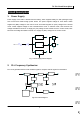
1) PLL Circuit
Step frequency of PLL can be 2.5 KHz, 5.0 KHz or 6.25 KHz. A 16.8MHz reference oscillator signal is
divided at IC301 by a counter to generate a 2.5 KHz, 5.0 KHz or 6.25 KHz reference frequency. Output
signal from VCO is buffer amplified by Q301 and divided at IC301 by a frequency divider. The divided
signal is compared with 2.5 KHz, 5.0 KHz or 6.25 KHz reference signal in the phase comparator of IC301.
The output signal from phase comparator is filtered through a low pass filter to generate a level D.C., and
the level D.C. controls oscillator frequency by controlling VCO.
2) VCO
The operating frequency is generated by Q302 in transmit mode and by Q307 in receive mode.
Operating frequency generate a control voltage by phase comparator to control varactor diodes so that
the oscillator frequency is consistent with the MCU preset frequency(D301、D302、D303 and D304 in
transmit mode, and D307、D308、D309 and D310 in receive mode). T/R pin is set high level in receive
mode, and low level in transmit mode. The output from Q302 and Q307 is amplified by Q304 and sent to
buffer amplifier.
3) Unlock Detector
An unlock condition appears if low level appears at MUXOUT pin of IC301. Transmission is forbidden if
this condition is detected by microprocessor.
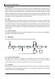
3. Receiver
The receiver utilizes double conversion superheterodyne (UHF)/(VHF).
Fig. 3 Receiver Section Configuration
1) Front-end RF Amplifier
The signal from antenna is amplified at RF amplifier (Q207) after passing through a
transmit/receive circuit and a band pass filter. Before passing the first mixer, the amplified
signal is filtered through another band pass filter to remove unwanted signals.
2) First Mixer
The signal from RF amplifier is mixed with the first local from PLL frequency synthesizer circuit at the fix
mixer (IC202) to create a 49.95MHz first IF signal. The first IF signal is then fed through a crystal filter
(XF203) to further remove unwanted signals.