HCTBLE42S1D Specification nRF51822 2.4GHz Bluetooth Module BLE4.
Chapter 1 Overview 1.1 Introduction HCTBLE42S1D is a small-sized SMD Bluetooth module developed based on nRF51822 produced by Nordic of Norway. It uses a 16Mhz industrial grade crystal to ensure its industrial characteristics and stability. nRF51822 comes with high-performance ARM CORTEX-M0 core and Bluetooth 4.2 radio frequency transceiver and protocol stack, and has rich peripheral resources such as UART, I2C, SPI, ADC, DMA, and PWM. This module redeveloped some IO ports.
2.1 Working parameter Range Parameters Operating Voltage(V) Min Standard 1.8 3.3 Note Max 3.6 ≥3.3V be able to stable output Output level(V) 3.0 Using 5V TTL risk of burn Working Temperature(℃) -40 - Working Frequency(MHz) 2379 2430 Emission +85 2496 14 Instant power consumption current(mA) Power Consumption Receive current(mA) 12 Sleep current 1 Software (μA) Max Transmit power(dBm) Receiving sensitivity(dBm) Parameters Reference distance shut down 0 -95.4 -96.
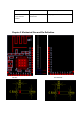
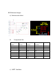
Antenna interface PCB Module Full-duplex communication transmission PCB Antenna,Equivalent resistance 50Ω serial Only supports 115200 baud rate method Chapter 3 Mechanical Size and Pin Definition TOP PAD BOTTOM PAD
Pin No.
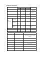
4.2 Antenna designs a) Antenna size chart b) Component list Serial Tag Device Device number number package parameters 1 C6 0402 4.7PF 2 C7 0402 1.2PF 3 C8 0402 0.1PF 4 C9 0402 47NF 5 C10 0402 2.2NF 6 L1 0402 3.6nH 7 L2 0402 4.
The UART interface provides two signals. TXD and RXD pins are used for data, fixed baud rate, support 115200bps. 4.3 Hardware Design 1. It is recommended to use a DC stabilized power supply to power the module. The ripple factor of the power supply should be as small as possible and the module should be reliably grounded; 2. Please pay attention to the correct connection of the positive and negative poles of the power supply, such as reverse connection may cause permanent damage to the module; 3.
5. When designing the power supply circuit for the module, it is often recommended to reserve more than 30% of the margin, as the whole machine is conducive to long-term stable work; 6. The module should be far away from the parts with large electromagnetic interference such as power supply, transformer, high-frequency wiring; 7. High-frequency digital routing, high-frequency analog routing, and power routing must be avoided under the module.
Chapter 5 Trouble Shooting 5.1 Transmission distance is not ideal 1. When there is a linear communication obstacle, the communication distance will be reduced correspondingly; 2. Temperature, humidity, and co-channel interference will increase communication packet loss rate; 3. The ground absorbs and reflects radio waves, and the test results near the ground are poor; 4. Sea water has a strong ability to absorb radio waves, so the test results at the seaside are poor; 5.
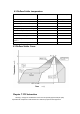
6.1 Reflow Solder temperature Profile Feature Sn-Pb Assembly Pb-Free Assembly Solder Paste Sn63/Pb37 Sn96.5/Ag3/Cu0.
This device complies with Part 15 of the FCC Rules. Operation is subject to the following two conditions: (1) this device may not cause harmful interference, and (2) this device must accept any interference received, including interference that may cause undesired operation. NOTE: This equipment has been tested and found to comply with the limits for a Class B digital device, pursuant to Part 15 of the FCC Rules.
8)Information on test modes and additional testing requirements The host manufacturer can use the software “ nRFgo ” for access to the test modes. Connected to the computer through the serial port of the host product, the channel and power controlling software provided by the applicant was used to control the operating channel as well as the output power level.