
Data Sheet
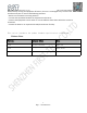

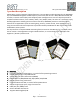

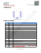
Table Of Contents

SHENZHEN FIRST TECHNOLOGY CO.,LTD FST50_04E WIFI DataSheet
http:// www.fst-tech.com
10
3.Module pin description
3.1 Module pin map
Pin distribution front view
3.2 Module pin description
Number
PIN
Function Description
1
PAD10
GPIO,High level is 3.3V
2
PAD11
GPIO,High level is 3.3V
3
RST
Reset pin; chip enable pin, low level chip is off, high level
works normally. Note: The module is pulled up by default
4
RXD1
Burn serial port,High level is equal to VCC
5
TXD1
Burn serial port,High level is equal to VCC
6
PAD4
GPIO,High level is 3.3V
7
PAD5
GPIO,High level is 3.3V
8
VCC
powered by,3.3V
9
PAD6
GPIO,High level is 3.3V
10
PAD7
GPIO,High level is 3.3V
11
PAD8
GPIO,High level is 3.3V
12
PAD9
GPIO,High level is 3.3V
13
GND
Ground
14
PAD_SEL
Mode selection, normally float or pull low. Note, do not pull
high.
15
PAD15
GPIO,High level is 3.3V
16
PAD_SEL1
Flashing Access 3.3V
17
PAD13
GPIO,High level is 3.3V
18
PAD12
GPIO,High level is 3.3V
19
RXD0
UART(RX),High level is equal to VCC , 10K pull-up resistor
must be connected externally