
Specifications


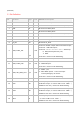


(TOP View)
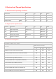
2.1 Pin Definition
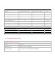
No.
Pin Name
Type
Level
Module Pin Description
1
GND
RF
RF Ground for WLAN_ANT1
2
NC
RF
NC(Reserved 2.4G / 5G RFPAD for WLAN_ANT1)
3
GND
RF
RF Ground for
WLAN_ANT1
4
GND
RF
RF Ground for
WLAN_ANT0
5
NC
RF
NC
(
Reserved
2.4G / 5G RF
PAD for
WLAN_ANT0)
6
GND
RF
RF Ground for
WLAN_ANT0
7
GND
RF
RF Ground for BT_ANT1
8
BT_RF1
RF
RF PAD for BT_ANT1
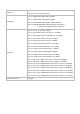
9
GPIO / UART_TXD
I/O
3.3V
Function1
、
GPIO15
,
output shall not be used as input
;
Function2
、
UART TXD output
;
Function3、BT Host Interface Select Boot strap:
0
:
USB (internal
pull Low by 10K)
1:UART
If not used,this Pin can be left floating .
10
GND
P
Ground for Power and I/O
11
GPIO / UART_RXD
I/O
3.3V
1
、
GPIO14
,
I/O
;
2、UART RXD input .
If not used,this Pin can be left floating .
12
GPIO / WL_Wake_Host
I/O
3.3V
1
、
GPIO1
,
I/O
;
2
、
Wlan Wake up Host
,
Active Low
output
,
internal pull high by 10K resistor.
If not used
,
this Pin can be left floating .
13
GND
P
Ground for Power and I/O
14
SSTX-
AO
USB3.0 SuperSpeed Device Interface TX differential pair,
DC blocked output(to connect USB 3.0 Host“
SSRX-
”)
If USB3.0 is not used
,
this Pin can be left floating .
15
SSTX+
AO
USB3.0 SuperSpeed Device Interface TX differential pair,
DC blocked output(to connect USB 3.0 Host“
SSRX+
”)
If USB3.0 is not used
,
this Pin can be left floating .
16
SSRX-
AI
USB3.0 SuperSpeed Device Interface RX differential pair
(to connect USB 3.0 Host“SSTX-”)
If USB3.0 is not used,this Pin can be left floating .