
Data Sheet

FSC‐BT630Datasheet
ShenzhenFeasycomTechnologyCo.,Ltdwww.feasycom.com
‐9‐
4.2Reset
Themodulemayberesetfromseveralsources:Power‐onReset(POR),LowlevelonthenRESETPin(nRST),Watchdog
time‐outreset(WDT),WakeupfromSystemOFFmodereset,Brown‐outresetorSoftwareReset(SYSRESETREQ,CPU
Reset,CHIPRST).
TheRESETpinisanactivelowresetandisinternallyfilteredusingtheinternallowfrequencyclockoscillator.Areset
willbeperformedbetween1.5and4.0msfollowingRESETbeingactive.ItisrecommendedthatRESETbeappliedfora
periodgreaterthan5ms.
At reset the digital I/O pins are set to inputs for bi‐directional pins and outputs are tri‐state. The PIOs have weak
pull‐ups.
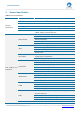
Table3:NRSTpincharacteristics
Parameter Conditions Min Typ Max Unit
R
PU
‐ Weakpull‐upequivalentresistor
(1)
VIN=VSS 30 40 50 KΩ
V
F(NRST)
(2)
‐ NRSTInputfilteredpulse ‐ ‐ 100 ns
V
NF(NRST)
(2)
‐ NRSTInputnotfilteredpulse VDD>1.2V 300‐ ‐ ns
T
NRST_OUT
‐ Generatedresetpulseduration InternalResetsource 20 ‐ ‐ μs
V
POF
‐ Nominalpowerlevelwarning
thresholds(fallingsupplyvoltage).
LevelsareconfigurablebetweenMin.and
Max.in100mVincrements.
1.7 2.8 V
V
BOR,OFF
‐ Brownoutresetvoltagerange
SYSTEMOFFmode
1.2 1.7 V
V
BOR,ON
‐ Brownoutresetvoltagerange
SYSTEMONmode
1.5 1.7 V
1.Thepull‐upisdesignedwithatrueresistanceinserieswithaswitchablePMOS.ThisPMOScontributiontotheseries
resistancemustbeminimum(~10%order).
2.Guaranteedbydesign.
1.Theresetnetworkprotectsthedeviceagainstparasiticresets.
2.TheusermustensurethatthelevelontheNRSTpincangobelowtheVIL(NRST)maxlevelspecifiedin
NRSTpincharacteristics.Otherwisetheresetisnottakenintoaccountbythedevice.
4.3GeneralPurposeAnalogIO
TheADCisadifferentialsuccessiveapproximationregister(SAR)analog‐to‐digitalconverter.
ListedherearethemainfeaturesofSAADC:
8/10/12‐bitresolution,14‐bitresolutionwithoversampling
Uptoeightinputchannels