
Data Sheet

FSC‐BT630Datasheet
ShenzhenFeasycomTechnologyCo.,Ltdwww.feasycom.com
‐31‐
9.3LayoutGuidelines(ExternalAntenna)
PlacementandPCBlayout arecriticaltooptimize the performancesofamodulewithouton‐boardantennadesigns.
Thetracefromtheantennaportofthemoduletoanexternalantennashouldbe50andmustbeasshortaspossible
toavoidanyinterferenceintothetransceiverofthe
module.ThelocationoftheexternalantennaandRF‐INportof
themoduleshouldbekept awayfroman ynoisesources anddigitaltraces.Amatching networkmight be neededin
betweentheexternalantennaandRF‐INporttobettermatchtheimpedancetominimizethereturnloss.
As
indicatedinFigure46below,RFcriticalcircuitsofthemoduleshouldbeclearlyseparatedfromanydigitalcircuitson
thesystemboard.AllRFcircuitsinthemoduleareclosetotheantennaport.Themodule, then,shouldbeplacedin
thiswaythatmoduledigitalparttowardsyour
digitalsectionofthesystemPCB.
9.3.1AntennaConnectionandGroundingPlaneDesign
Generaldesignrecommendationsare:
Thelengthofthetraceorconnectionlineshouldbekeptasshortaspossible.
Distance between connection and ground area on the top layer should at least be as large as the dielectri c
thickness.
RoutingtheRFclosetodigitalsectionsofthesystemboardshouldbeavoided.
To reduce signal reflections, sharp angles in the routing of the micro strip line should be avoided. Chamfers or
fillets are preferred for rectangular routing; 45‐degree routing is preferred over Manhattan style 90‐degree
routing.
RoutingoftheRF‐connectionunderneaththemoduleshouldbeavoided.Thedistanceofthemicrostriplinetothe
groundplaneonthebottomsideofthereceiverisverysmallandhashugetolerances.Therefore,theimpedance
ofthispartofthetracecannotbecontrolled.
Useasmanyviasaspossibletoconnectthegroundplanes.
10.PRODUCTPACKAGINGINFORMATION
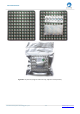
10.1DefaultPacking
a,Trayvacuum
b,TrayDimension:180mm*195mm