
Data Sheet

FSC‐BT630Datasheet
ShenzhenFeasycomTechnologyCo.,Ltdwww.feasycom.com
‐30‐
8.MECHANICALDETAILS
8.1MechanicalDetails
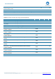
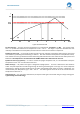
Dimension:10mm(W)x11.9mm(L)x1.7mm(H)Tolerance:±0.1mm
Modulesize:10mmX11.9mmToleranc e:±0.1mm
Padsize:0.9mmX0.6mmToleran ce:±0.1mm
Padpitch:1.1mmToleran ce: ±0.1mm
9.HARDWAREINTEGRATIONSUGGESTIONS
9.1SolderingRecommendations
FSC‐BT630iscompatiblewithindustrialstandardreflowprofileforPb‐freesolders.Thereflowprofileusedisdependent
on the thermal mass of the entire populated PCB, heat transfer efficiency of the oven and particular type of solder
pasteused.Consultthedatasheetofparticularsolderpasteforprofileconfigurations.
Feasycomwillgivefollowingrecommendationsforsolderingthemoduletoensurereliablesolderjointandoperationof
the module after soldering. Since the profile used is process and layout dependent, the optimum profile should be
studiedcasebycase.Thusfollowingrecommendationshouldbetakenasastartingpointguide.
9.2LayoutGuidelines(InternalAntenna)
Itisstronglyrecommendedtousegoodlayoutpracticestoensureproperoperationofthemodule.Placingcopperor
anymetalnearantennadeterioratesitsoperationbyhavingeffectonthematchingproperties.Metalshieldaroundthe
antenna will prevent the radiation and thus metal case should not be used with
the module. Use grounding vias
separated max 3 mmapartattheedgeof grounding areastoprevent RF penetratinginsidethePCBandcausing an
unintentionalresonator.UseGNDviasallaroundthePCBedges.
Themotherboardshouldhavenobareconductorsorviasinthisrestrictedarea,
becauseitisnotcoveredbystopmask
print.Alsonocopper(planes,tracesorvias)areallowedinthisarea,becauseofmismatchingtheon‐boardantenna.
FollowingrecommendationshelpstoavoidEMCproblemsarisinginthedesign.Notethateachdesignisuniqueandthe
followinglistdonot
considerallbasicdesignrulessuchasavoidingcapacitivecouplingbetweensignallines.Following
listisaimedtoavoidEMCproblemscausedbyRFpartofthemodule.Usegoodconsiderationtoavoidproblemsarising
fromdigitalsignalsinthedesign.
Ensurethatsignallineshavereturnpathsasshort
aspossible.Forexampleifasignalgoestoaninnerlayerthrougha
via, always use ground vias around it. Locate them tightly and symmetrically around the signal vias. Routing of any
sensitivesignalsshouldbedoneintheinnerlayersofthePCB.Sensitivetracesshouldhaveaground
areaaboveand
under the line. If this is not possible, make sure that the return path is short by other means (for example using a
groundlinenexttothesignalline).