
Data Sheet

FSC‐BT630Datasheet
ShenzhenFeasycomTechnologyCo.,Ltdwww.feasycom.com
‐16‐
corresponding pins for a 100mS period. The total average PIO pin output current is defined as the average current
valueflowingthroughallofthecorrespondingpinsfora100mSperiod.The maximumoutputcurrentisdefinedasthe
valueofthepeakcurrentflowingthroughanyoneofthecorresponding
pins.
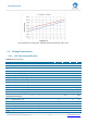
Table5:AbsoluteMaximumRating
Parameter Min Max Unit
Supplyvoltages
VDD ‐0.3 +3.9V V
VSS 0V V
I/Opinvoltage
V
I/O
,VDD≤3.6V ‐0.3 VDD+0.3 V
V
I/O
,VDD>3.6V ‐0.3 3.9V V
NFCantennapincurrent
I
NFC1/2
80 mA
Radio
RFinputlevel 10 dBm
Environmental
Storagetemperature ‐40 +125 °C
5.2RecommendedOperatingConditions
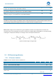
Table6:RecommendedOperatingConditions
Parameter Min Type Max Unit
V
DD
‐Supplyvoltage,independentofDCDCenable 1.7 3.0 3.6 V
t
R_VDD
‐ Supplyrisetime(0Vto1.7V) 60 mS
T
A
‐ OperatingTemperature‐40 25 +85 °C
Important:
Theon‐chippower‐onresetcircuitrymaynotfunctionproperlyforrisetimeslongerthanthespecifiedmaximum.
5.3Input/outputTerminalCharacteristics
Table7:GPIOElectricalSpecification
Parameter Min Type Max Unit
V
IH
‐ InputHighVoltage 0.7xVDD‐ VDD V
V
IL
‐ InputLowVoltage VSS ‐ 0.3xVDD V
V
OH,HDH
‐ Outputhighvoltage,standarddrive,0.5mA,VDD≥1.7 VDD‐0.4‐ VDD V
V
OH,HDH
‐ Outputhighvoltage,highdrive,5mA,VDD>=2.7V VDD‐0.4 ‐ VDD V
V
OH,HDL
‐ Outputhighvoltage,highdrive,3mA,VDD>=1.7V VDD‐0.4‐ VDD V
V
OL,SD
‐ Outputlowvoltage,standarddrive,0.5mA,VDD≥1.7 VSS ‐ VSS+0.4 V
V
OL,HDH
‐ Outputlowvoltage,highdrive,5mA,VDD>=2.7V VSS‐VSS+0.4 V