FSC‐BT630 Datasheet FSC‐BT630 Bluetooth low energy 4.2 and 5 Specifications Module Datasheet Version 1.0 Shenzhen Feasycom Technology Co.,Ltd ‐1‐ www.feasycom.
FSC‐BT630 Datasheet Copyright © 2013‐2017 Feasycom Technology. All Rights Reserved. Feasycom Technology reserves the right to make corrections, modifications, and other changes to its products, documentation and services at anytime. Customers should obtain the newest relevant information before placing orders. To minimize customer product risks, customers should provide adequate design and operating safeguards.
FSC‐BT630 Datasheet 1. INTRODUCTION Overview Type 2 near field communication (NFC‐A) tag with wakeup‐on‐field and touch‐to‐pair capabilities FSC‐BT630 is a wireless microcontroller (MCU) targeting Bluetooth 4.2 and Bluetooth 5 low energy applications.
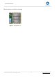
FSC‐BT630 Datasheet Module picture as below showing Figure 1: FSC‐BT630 Picture Shenzhen Feasycom Technology Co.,Ltd ‐4‐ www.feasycom.
FSC‐BT630 Datasheet 2. General Specification Table 1: General Specifications Categories Wireless Specification Features Implementation Bluetooth Version Bluetooth low energy (BLE) 4.2 and 5 Specifications Frequency 2.402 ‐ 2.
FSC‐BT630 Datasheet listen mode operation Bit rate 106 kbps 3 SPI instances(configurable from GPIO total) SPI SPI Slave and SPI Master Bit rates for SPI Slave and Master ‐ 8 Mbps Temperature sensor Temperature range is greater than or equal to operating temperature of the device Resolution is 0.
FSC‐BT630 Datasheet 3. 3.1 HARDWARE SPECIFICATION PIN Definition Descriptions Table 2: Pin definition Pin Pin Name Type Pin Descriptions Notes 1 UART_TX O UART Data output Note 1 2 UART_RX I UART Data input Note 1 3 PIO0/I2C_SDA I/O Programmable input/output line Note 2,3 4 PIO1/I2C_SCL I/O Programmable input/output line Note 2,3 5 PIO2/AIO0/TRAN I/O Programmable input/output line Alternative Function 1: Analogue programmable I/O line.
FSC‐BT630 Datasheet Alternative Function 2: NFC2 18 PIO10/STATUS/NFC1 I/O Programmable input/output line Alternative Function 1: BT Status Alternative Function 2: NFC1 19 GND Vss Power Ground 20 EXT_ANT O RF signal output . Note 8 Note 9 Module Pin Notes: Note 1 For customized module, this pin can be work as I/O Interface. Note 2 Note 5 I2C/PWM/SPI/PDM/UART(CTS/RTS) with EasyDMA (Support accomplishing the port mapping to other spare I/O Interface via modifying the firmware.
FSC‐BT630 Datasheet 4.2 Reset The module may be reset from several sources: Power‐on Reset (POR), Low level on the nRESET Pin (nRST), Watchdog time‐out reset (WDT), Wakeup from System OFF mode reset , Brown‐out reset or Software Reset(SYSRESETREQ, CPU Reset, CHIPRST). The RESET pin is an active low reset and is internally filtered using the internal low frequency clock oscillator. A reset will be performed between 1.5 and 4.0ms following RESET being active.
FSC‐BT630 Datasheet • One channel per single‐ended input and two channels per differential input • Scan mode can be configured with both single‐ended channels and differential channels. Full scale input range (0 to VDD) Sampling triggered via a task from software or a PPI channel for full flexibility on sample frequency source from low power 32.768kHz RTC or more accurate 1/16MHz Timers One‐shot conversion mode to sample a single channel Scan mode to sample a series of channels in sequence.
FSC‐BT630 Datasheet 8, 16 and 24‐bit sample width Low‐jitter Master Clock generator Various sample rates 4.6 SPI Interfaces The SPI master provides a simple CPU interface which includes a TXD register for sending data and an RXD register for receiving data. This section is added for legacy support for now. The TXD and RXD registers are double-buffered to enable some degree of uninterrupted data flow in and out of the SPI master. The SPI master does not implement support for chip select directly.
FSC‐BT630 Datasheet This is a standard UART interface for communicating with other serial devices. The UART interface provides a simple mechanism for communicating with other serial devices using the RS232 protocol. When the module is connected to another digital device, UART_RX and UART_TX transfer data between the two devices. The remaining two signals, UART_CTS and UART_RTS, can be used to implement RS232 hardware flow control where both are active low indicators. This module output is at 3.
FSC‐BT630 Datasheet corruption if two or more masters attempt to control the bus simultaneously. Data is transferred between a Master and a Slave synchronously to SCL on the SDA line on a byte‐by‐byte basis. Each data byte is 8‐bit long. There is one SCL clock pulse for each data bit with the MSB being transmitted first. An acknowledge bit follows each transferred byte.
FSC‐BT630 Datasheet HW decimation filters The PDM module illustrated The PDM module illustrated is interfacing up to two digital microphones with the PDM interface. It implements EasyDMA, which relieves real‐time requirements associated with controlling the PDM slave from a low priority CPU execution context. It also includes all the necessary digital filter elements to produce PCM samples. The PDM module allows continuous audio streaming. 4.10.
FSC‐BT630 Datasheet 4.11.2 NFCT antenna recommendations The NFCT antenna coil must be connected differential between NFC1 and NFC2 pins of the device. Two external capacitors should be used to tune the resonance of the antenna circuit to 13.56MHz. The required tuning capacitor value is given by the below equations: An antenna inductance of Lant = 2 μH will give tuning capacitors in the range of 130pF on each pin. For good performance, match the total capacitance on NFC1 and NFC2. 4.11.
FSC‐BT630 Datasheet corresponding pins for a 100mS period. The total average PIO pin output current is defined as the average current value flowing through all of the corresponding pins for a 100mS period. The maximum output current is defined as the value of the peak current flowing through any one of the corresponding pins. Table 5: Absolute Maximum Rating Parameter Min Max Unit ‐0.3 +3.9V V 0V V Supply voltages VDD VSS I/O pin voltage VI/O, VDD ≤3.6 V ‐0.3 VDD+0.3 V VI/O, VDD >3.6 V ‐0.
FSC‐BT630 Datasheet VOL,HDL ‐ Output low voltage, high drive, 3 mA, VDD >= 1.7 V VSS ‐ VSS+0.4 V IOL,SD ‐ ≥1.7 Current at VSS+0.4 V, output set low, standard drive, VDD 1 2 4 mA IOL,HDH ‐ 2.7 V Current at VSS+0.4 V, output set low, high drive, VDD >= 6 10 15 mA IOL,HDL ‐ 1.7 V Current at VSS+0.4 V, output set low, high drive, VDD >= 3 ‐ ‐ mA IOH,SD ‐ Current at VDD‐0.4 V, output set high, standard drive, VDD ≥1.7 1 2 4 mA IOH,HDH ‐ Current at VDD‐0.
FSC‐BT630 Datasheet GPIO drive strength vs Voltage, standard drive, VDD = 3.0 V GPIO drive strength vs Voltage, high drive, VDD = 3.0 V Max sink current vs Voltage, standard drive Max sink current vs Voltage, high drive Shenzhen Feasycom Technology Co., Ltd ‐18‐ www.feasycom.
FSC‐BT630 Datasheet Rise and fall time vs Temperature, 10%‐90%, 25pF load capacitance, VDD = 3.0 V 5.4 Analog Characteristics 5.4.1 ADC Electrical Specification Table 8: ADC characteristics Parameter Min Typ DNL ‐ Differential non‐linearity, 10‐bit resolution ‐0.95 <1 ‐ LSB INL ‐ Integral non‐linearity, 10‐bit resolution ‐ 1 ‐ LSB ‐ +‐2 ‐ LSB ‐ 0.
FSC‐BT630 Datasheet ENOB ‐ Effective number of bits, differential mode, 12‐bit resolution, 1/1 gain, 3 μs acquisition time, crystal HFCLK, 200 ksps ‐ 9 ‐ Bit SNDR ‐ Peak signal to noise and distortion ratio, differential mode, 12‐ bit resolution, 1/1 gain, 3 μs acquisition time, crystal HFCLK, 200ksps ‐ 56 ‐ dB SFDR ‐ Spurious free dynamic range, differential mode, 12‐bit resolution, 1/1 gain, 3 μs acquisition time, crystal HFCLK, 200ksps ‐ 70 ‐ dBc RLADDER ‐ Ladder resistance ‐ 160 ‐ kΩ
FSC‐BT630 Datasheet tSPI,START,CL ‐ Time from writing TXD register to transmission started, constant latency mode ‐ 1 ‐ uS a:Higher bit rates may require GPIOs to be set as High Drive, see GPIO chapter for more details. b:The actual maximum data rate depends on the slave's CLK to MISO and MOSI setup and hold timings.
FSC‐BT630 Datasheet Constant latency mode a:Higher bit rates may require GPIOs to be set as High Drive, see GPIO chapter for more details. b:The actual maximum data rate depends on the slave's CLK to MISO and MOSI setup and hold timings.
FSC‐BT630 Datasheet tI2C,START,CL ‐ Time from STARTRX/STARTTX task to transmission started, Constant latency mode ‐ 1.5 ‐ μS a: Higher bit rates or stronger pull‐ups may require GPIOs to be set as High Drive, see GPIO chapter for more details.
FSC‐BT630 Datasheet Recommended TWIM pullup value vs. line capacitance • The I2C specification allows a line capacitance of 400 pF at most. • FSC‐BT630 internal pullup has a fixed value of typ. 13 kOhm, see RPU in the GPIO chapter. 5.6.
FSC‐BT630 Datasheet low), 100 kbps tI2C,HD_STA,400kbps‐ I2C slave hold time from for START condition (SDA low to SCL low), 400 kbps 1300 ‐ ‐ nS tI2C,SU_STO,100kbps ‐ 100 kbps I2C slave setup time from SCL high to STOP condition, 5200 ‐ ‐ nS tI2C,SU_STO,400kbps ‐ 400 kbps I2C slave setup time from SCL high to STOP condition, ‐ ‐ nS 4700 ‐ nS 1300 ‐ nS Min Typ Max Unit 1300 tI2C,BUF,100kbps ‐ I2C slave bus free time between STOP and START conditions, 100 kbps ‐ tI2C,BUF,400kbps ‐
FSC‐BT630 Datasheet PDM module active current, stereo operationa IPDM,stereo ‐ fPDM,CLK ‐ PDM clock speed tPDM,JITTER ‐ Jitter in PDM clock output TdPDM,CLK ‐ PDM clock duty cycle tPDM,DATA ‐ Decimation filter delay ‐ 1.4 ‐ mA ‐ 1.032 ‐ MHz ‐ ‐ 20 nS 40 50 60 % ‐ ‐ 5 ms tPDM,cv ‐ Allowed clock edge to data valid ‐ ‐ 125 nS tPDM,ci ‐ Allowed (other) clock edge to data invalid 0 ‐ ‐ nS tPDM,s ‐ Data setup time at fPDM,CLK=1.
FSC‐BT630 Datasheet ‐ 100 ‐ nA ‐ 480 ‐ uA Rin_min ‐ Minimum input resistance when regulating voltage swing ‐ ‐ 40 Ω Rin_max ‐ Maximum input resistance when regulating voltage swing 1.
FSC‐BT630 Datasheet 6. MSL & ESD Table 24: MSL and ESD Parameter Value MSL (moisture sensitivity level) MSL 1 ESD grade: ESD HBM (human body model): 2KV ESD HBM (human body model): 500V 7. RECOMMENDED TEMPERATURE REFLOW PROFILE Prior to any reflow, it is important to ensure the modules were packaged to prevent moisture absorption. New packages contain desiccate (to absorb moisture) and a humidity indicator card to display the level maintained during storage and shipment.
FSC‐BT630 Datasheet Typical Lead‐free Re‐flow Pre‐heat zone (A) — This zone raises the temperature at a controlled rate, typically 0.5 – 2 C/s. The purpose of this zone is to preheat the PCB board and components to 120 ~ 150 C. This stage is required to distribute the heat uniformly to the PCB board and completely remove solvent to reduce the heat shock to components.
FSC‐BT630 Datasheet MECHANICAL DETAILS 8. 8.1 9. 9.1 Mechanical Details Dimension: 10mm(W) x 11.9mm(L) x 1.7mm(H) Tolerance: ±0.1mm Module size: 10mm X 11.9mm Tolerance: ±0.1mm Pad size: 0.9mmX0.6mm Tolerance: ±0.1mm Pad pitch: 1.1mm Tolerance: ±0.1mm HARDWARE INTEGRATION SUGGESTIONS Soldering Recommendations FSC‐BT630 is compatible with industrial standard reflow profile for Pb‐free solders.
FSC‐BT630 Datasheet 9.3 Layout Guidelines(External Antenna) Placement and PCB layout are critical to optimize the performances of a module without on‐board antenna designs. The trace from the antenna port of the module to an external antenna should be 50 and must be as short as possible to avoid any interference into the transceiver of the module. The location of the external antenna and RF‐IN port of the module should be kept away from any noise sources and digital traces.
FSC‐BT630 Datasheet Figure 49: Tray vacuum (Image for reference only, subject to actual product) Shenzhen Feasycom Technology Co., Ltd ‐32‐ www.feasycom.
FSC‐BT630 Datasheet FCC Statement 15.19 1. This device complies with Part 15 of the FCC Rules. Operation is subject to the following two conditions: (1) This device may not cause harmful interference. (2) This device must accept any interference received, including interference that may cause undesired operation. 15.21 Note: The grantee is not responsible for any changes or modifications not expressly approved by the party responsible for compliance.
FSC‐BT630 Datasheet observed to ensure compliance with current FCC / IC RF exposure guidelines. ⚫ The final host / module combination may also need to be evaluated against the FCC Part 15B criteria for unintentional radiators in order to be properly authorized for operation as a Part 15 digital device. ⚫ This Module is full modular approval, it is limited to OEM installation ONLY. ⚫ The module is limited to installation in mobile application.