
Data Sheet

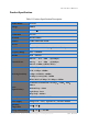

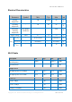

Table Of Contents

Copyright © 2018 Shenzhen Ai-Thinker Technology Co., Ltd All Rights Reserved
第 6 页 共 14
页
Table 2.2 Pin function description
No.
Pin Name
Functional Description
1
RST
Reset Pin, Active Low
2
ADC
AD conversion, Input voltage range 0~1V, the value range
is 0~1024.
3
EN
Chip Enabled Pin, Active High
4
IO16
Connect with RST pin to wake up Deep Sleep
5
IO14
GPIO14; HSPI_CLK
6
IO12
GPIO12; HSPI_MISO
7
IO13
GPIO13; HSPI_MOSI; UART0_CTS
8
VCC
Module power supply pin, Voltage 3.0V ~ 3.6V