
Programming instructions
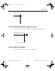

CMOS
Multisim Component Reference Guide 7-20 ni.com
7.2.39 4035 (4-bit Shift Register)
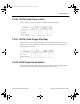
Following are two shift register truth tables.
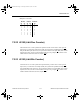
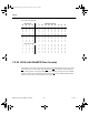
Serial operation first stage:
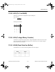
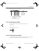
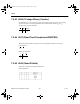
Parallel operation:
The 4035 device is a fully synchronous edge-triggered 4-bit shift register with a clock input
(CP), four synchronous parallel data inputs (P0 to P3), two synchronous serial data inputs
(J, K
), a synchronous parallel enable input (PE), buffered parallel outputs from all 4-bit
positions (O0 to O3), a true/complement input (T/C
) and an overriding asynchronous
master reset input (MR).
INPUTS OUTPUT
CP J K
MR
O
0
+1
MODE OF OPERATION
1 1 0 1 D flip-flop
0 0 0 0 D flip-flop
100 O
0
toggle
010 O
0
no change
XXX1 0 reset
CP
INPUTS OUTPUTS
P0 P1 P2 P3 O0 O1 O2 O3
00000000
11111111
= positive-going transition
1 = HIGH state (the more positive voltage)
0 = LOW state (the less positive voltage)
X = state is immaterial
ComponentRef.book Page 20 Thursday, December 7, 2006 10:12 AM